Zilog Z16C30 User Manual
Page 139
7-11
Z16C30 USC
®
U
SER
'
S
M
ANUAL
Z
ILOG
UM97USC0100
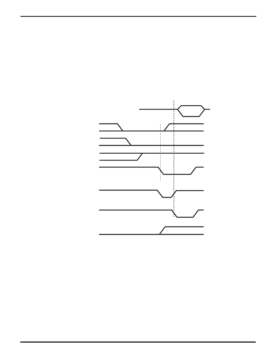
Figure 7-6 shows an interrupt acknowledge cycle that’s
signalled by /SITACK, on a bus with separate address and
data lines. (As before there are two subcases of this kind
of cycle, depending on whether the host processor uses
/DS or /RD signalling. Since the timing is identical for either
strobe, Figure 7-6 simply shows a trace labelled “/DS or
/RD”.)
Here the channel freezes its internal interrupt state in
response to a falling edge on /SITACK; again, if it is
requesting an interrupt it forces its IEO output low regard-
less of the state of IEI, and starts resolving its internal
interrupt priorities.
In this mode /SITACK must stay low until after /DS or /RD
goes low, and IEI must be valid for a specified setup time
before /DS or /RD goes low. (The falling edge of /DS or /RD
may have to be delayed to guarantee this.) If IEI is high and
the channel is requesting an interrupt, it responds to /DS or
/RD by setting the IUS bit of its highest priority requesting
type of interrupt, driving a vector onto the AD7-0 pins, and
driving /WAIT//RDY appropriately to signal when the vec-
tor is valid. If IEI is low at the leading/falling edge on /DS or
/RD, and/or if the channel is not requesting an interrupt, it
doesn’t respond to the cycle.
AD15-AD0
vector
/SITACK
IEO
IEI
/DS OR /RD
/WAIT//RDY
(as Wait)
/WAIT//RDY
(as Ack)
/INT
Figure 7-6. An Interrupt Acknowledge Cycle signalled by /SITACK, on a Non-Multiplexed Bus
UM009402-0201