Zilog Z16C30 User Manual
Page 199
B-5
Z16C30 USC
®
U
SER
'
S
M
ANUAL
Z
ILOG
UM97USC0100
Q:
With the DPLL, what is the purpose of multiple possi-
bilities of divisors?
A:
The DPLL is used to recover clock information from a
data stream with NRZI or Biphase encoding. The
higher the divisor, the less instantaneous jitter there is
in the recovered clock. But the price you pay is a lower
maximum data rate. Thus the USC family allows the
designer to trade off data rate for jitter in the recovered
clock.
Q:
When using a USC family device in HDLC Loop mode,
the DPLL is used to clock receive data. Can the DPLL
be used to retransmit the data?
A:
Certainly, just select the source of the transmit clock as
the DPLL in the Clock Mode Control Register (CMCR).
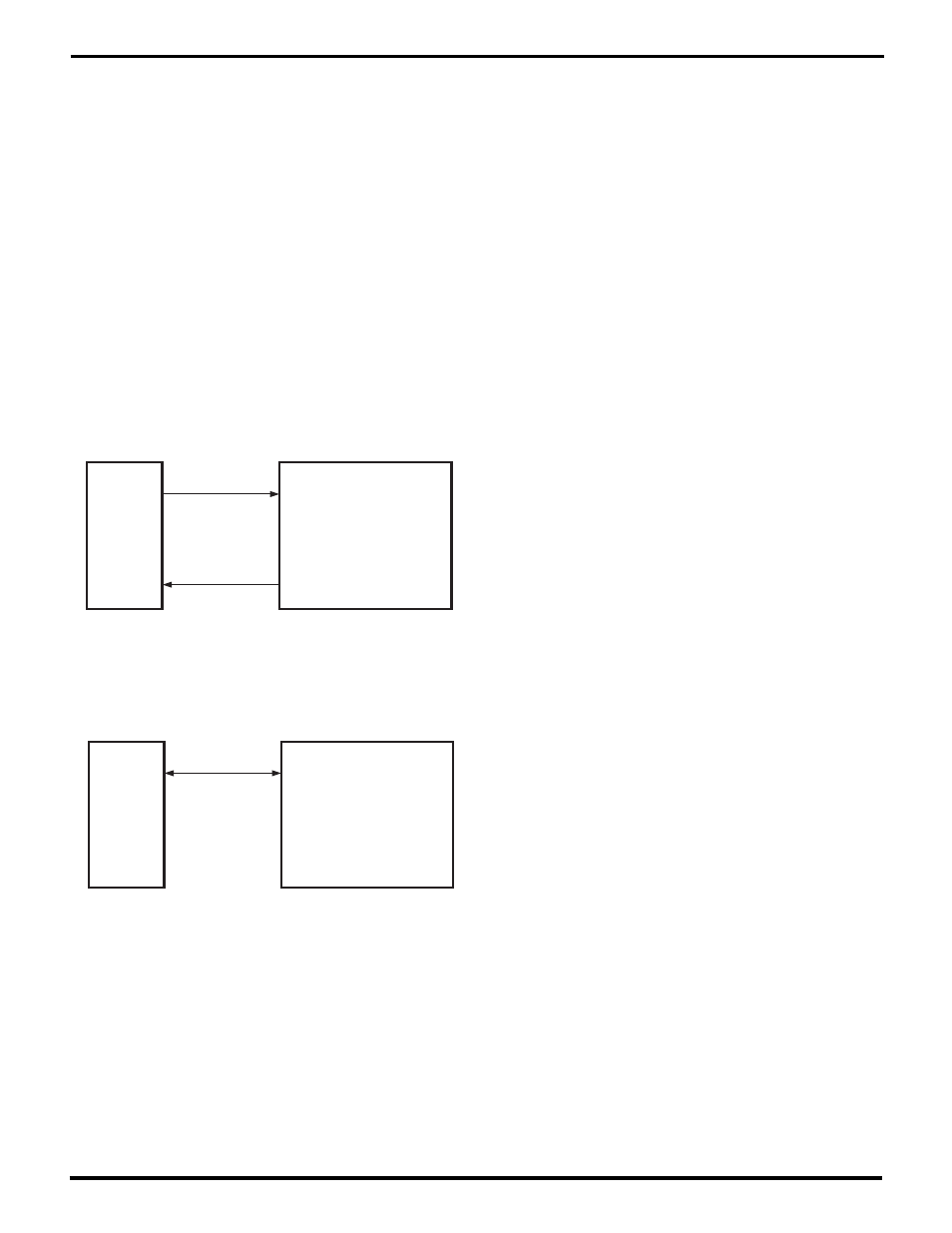
Q:
Can a USC family device perform HDLC half-duplex
transfers using separate TxD and RxD lines (as illus-
trated below)?
A:
Yes, this is all software driven.
Q:
Can a USC family device perform HDLC half-duplex
transfers by using only one line (as illustrated below)?
A:
Setting the RTMode field (D9-D8) of the CCAR to 10
will allow the system to transmit in half-duplex over the
TxD pin. This mode is called “pin controlled local
loopback”. When the TxDMode field (D7-D6) of IOCR
is 00 (Totem-pole setting) data is transmitted from the
USC family device to an external device via the TxD
pin. At the same time, this data is looped back into the
internal receive data input. For the device to receive
data, the TxDMode field (D7-D6) should be set to 01,
selecting the high-impedance state for the TxD driver.
Now, the incoming data from the external device will
be routed to the internal receive data input of the USC
family device. In both cases, the modem hand shaking
signals (/CTS, /DCD) will control who transmits and
who receives.
Q:
In the configuration: asynchronous with 7-bits charac-
ter, can the USC family put 0’s in the upper/unused
bits?
A:
The USC family receiver puts the stop bit in the unused
bits of a byte. Thus they are one’s in the normal case
and zero’s in the case of a framing error.
Q:
Do USC family devices have a Recovery Time like the
Zilog Z8530 SCC does?
A:
No. The USC family does not have a recovery time. The
Bus Cycle Time (AC Spec #1) specifies the access
time of the device. The bus interface is asynchronous
and is similar to that of a static RAM.
Q:
Does the USC family limit the serial data rate with
respect to the CPU clock the way the SCC limits the
serial data rate to 1/4 of PCLK?
A:
No. The USC family does not limit the serial data rate
with respect to the speed of the CPU interface. The
parallel and serial portions of the device operate
asynchronously to each other.
Q:
Can USC family devices transmit and receive packets
that are composed of multiple chained buffers as well
as having the packets themselves chained together?
A:
Since the USC does not have on-chip DMA, the
composition of how the data is organized in memory is
independent of how data is written to or read from the
USC. The IUSC’s on-chip DMA is able to send and
receive messages composed of multiple buffers as
well as terminate a buffer at the end of the message.
TxD
IUSC
RxD
Transmission
Facility
TxD
IUSC
RxD
Transmission
Facility
UM009402-0201