7 pull-up resistors and unused pins, 8 the bus configuration register (bcr), 1 wait vs. ready selection – Zilog Z16C30 User Manual
Page 33: 2 bits and fields in the bcr
2-7
Z16C30 USC
®
U
SER
'
S
M
ANUAL
Z
ILOG
UM97USC0100
2.7 PULL-UP RESISTORS AND UNUSED PINS
All unused input pins should be pulled up, either by
connecting them directly to Vcc or with a resistor. This may
include /PITACK, /SITACK, IEI, and /ABORT.
Bi-directional pins should typically be pulled up with a
resistor of about 10K ohms, to allow the USC to drive them
as outputs. This may include /TxREQ, /RxREQ, /TxC, /RxC,
/CTS, and /DCD.
Tri-state output pins may need to be pulled up to protect
external logic from the effects of having a floating input.
Again, a resistor of about 10K ohms is recommended. This
may include /TxREQ, /RxREQ, TxD, and /INT.
2.8 THE BUS CONFIGURATION REGISTER (BCR)
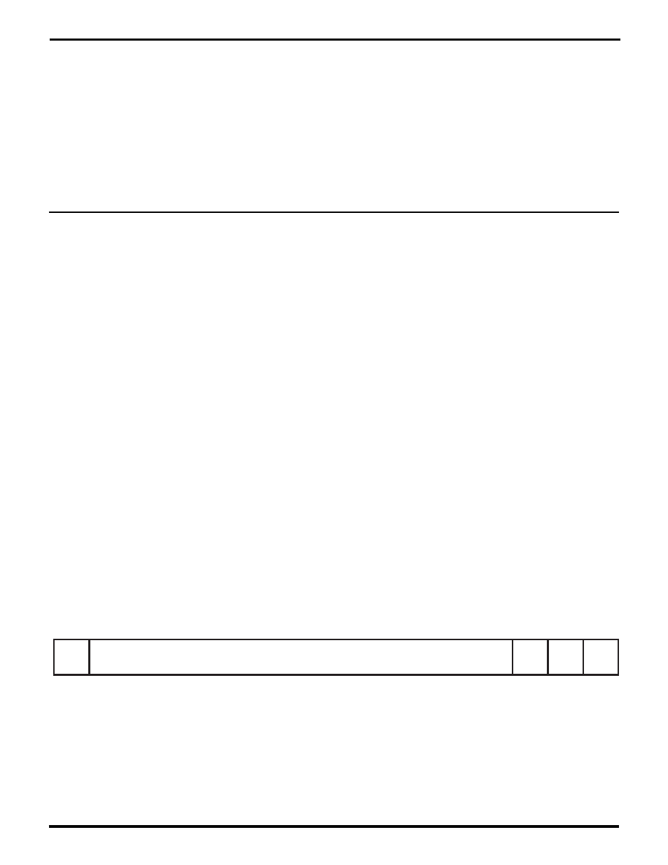
The BCR is a 16-bit register having the format shown in
Figure 2-7. All the bits in the BCR reset to zero. Software's
first access to the USC
™
after a hardware reset, must be a
write to the BCR. If the host processor handles 16-bit data,
and the data bus between it and the USC is at least 16 bits
wide, then the software’s initial access to the USC should
be a 16-bit write. This write can be to any address that
activates the /CS pin; the data will be placed in the BCR.
If the host can only write bytes to the USC, all data should
be transferred on the AD7-AD0 pins. In such a system,
pull-down resistors should be attached to the AD15-AD8
pins to ensure the state of these lines during the BCR write.
(AD15 may want to be pulled up instead of down, as
described in the section on the SepAd bit below.)
2.8.1 Wait vs. Ready Selection
The USC captures the state of the A//B pin when the
software writes the BCR. It uses this captured state after
the BCR write, such that if A//B was low, it drives the /WAIT
//RDY pin as an “acknowledge” (or inverted “ready”) signal
during register accesses and interrupt acknowledge cycles,
while if A//B was high, it drives the pin as a “wait” signal
during interrupt acknowledge cycles only. Therefore, soft-
ware should program the BCR at an address that corre-
sponds to the kind of slave-to-master handshaking used
on the host bus.
2.8.2 Bits and Fields in the BCR
SepAd
(Separate Address; BCR15): this bit should only be
written as 1 with 16-bit=0. This combination conditions the
USC to use AD7-AD0 for data and to take register address-
ing from AD13-AD8. In this mode the USC takes the Upper/
Lower byte indication (U//L) from AD8 and the register
address from AD13-AD9
With this interfacing technique, the BCR must be written at
an address such that AD13-AD8 are low/zero. Further,
AD15 must be high/one and AD14 must be low/zero when
software writes the BCR. The designer can ensure this by
connecting AD15 and AD14 to more-significant address
lines and writing the BCR at an appropriate address.
Alternatively, the designer can ensure this by connecting
a pull-up resistor to AD15 and a pulldown resistor to AD14.
This mode is useful with a non-multiplexed bus, to avoid
making the software write a register address to CCAR
before each register access. In this mode the USC cap-
tures the state of AD13-AD8 on each leading/falling edge
on /DS, /RD, or /WR. But software can still program SepAd=1
(with 16-bit=0) when the USC has detected early activity
on /AS. In this case the USC captures addressing from
AD13-AD8 on each rising edge of /AS, rather than from the
low-order AD lines as would be true with SepAd=0.
Reserved
SepAd
16-Bit
2Pulse
IACK
SRight
A
14
13
12
11
10
9
8
7
6
5
4
3
2
1
0
15
Figure 2-7. The USC’s Bus Configuration Register (BCR)
UM009402-0201