Zilog Z16C30 User Manual
Page 29
2-3
Z16C30 USC
®
U
SER
'
S
M
ANUAL
Z
ILOG
UM97USC0100
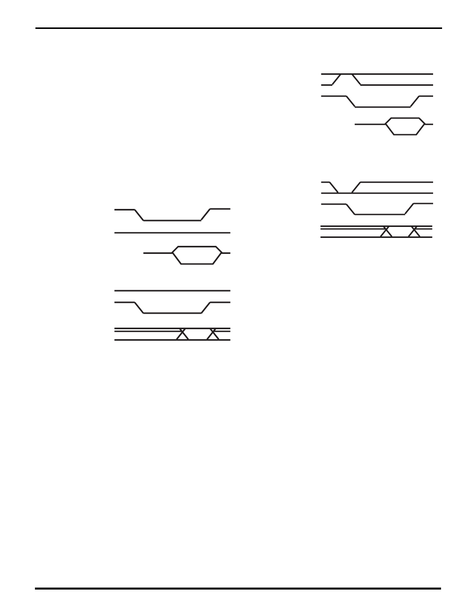
2.3 READ/WRITE DATA STROBES
Another difference among host buses is the way in which
read and write cycles are signalled and differentiated.
Figures 2-4 and 2-5 show two standard methods sup-
ported by the USC. In Figure 2-4, the bus includes sepa-
rate strobe lines for read and write cycles, commonly
called /RD and /WR. In Figure 2-5, the bus includes a data
strobe line, /DS, that goes low for both read and write
cycles, and a R//W line that differentiates read cycles from
writes. The USC includes pins for all four of these signals.
The two that match up with host bus signals should be
connected to those signals. The two unused pins should
be pulled up to a high level.
Read Operation:
Write Operation:
RD*
WR*
Data Bus
RD*
WR*
Data Bus
Figure 2-4. /RD and /WR Signaling
Read Operation:
Write Operation:
R//W
DS*
R//W
Data Bus (Slave)
Data Bus
DS*
Figure 2-5. R//W and /DS Signaling
There is no programmable option for the distinction be-
tween /RD-/WR and R//W-/DS operation. The USC simply
responds to either pair of lines, which is why it’s important
to pull up the unused pair. Also, the USC doesn’t demand
that the R//W line remain valid throughout the assertion of
/DS. It captures the state of R//W at the leading/falling edge
of /DS, so that R//W need only satisfy setup and hold times
with respect to this edge.
Only one among the bus signals /DS, /RD, /WR, and
/PITACK may be active at a time.
This prohibition also
includes /RxACKA, /RxACKB, /TxACKA, and /TxACKB
when these pins are used as DMA acknowledge signals.
(Chapter 5 covers DMA interfacing including the “ACK”
signals, and Chapter 6 describes the USC’s interrupt
features including /PITACK). If the USC detects more than
one of these inputs active simultaneously, it enters an
inactive state from which the only escape is via the /RESET
pin.
UM009402-0201