Zilog Z16C30 User Manual
Page 31
2-5
Z16C30 USC
®
U
SER
'
S
M
ANUAL
Z
ILOG
UM97USC0100
RD* or WR*
or DS*
WAIT*
ACK*
Ready
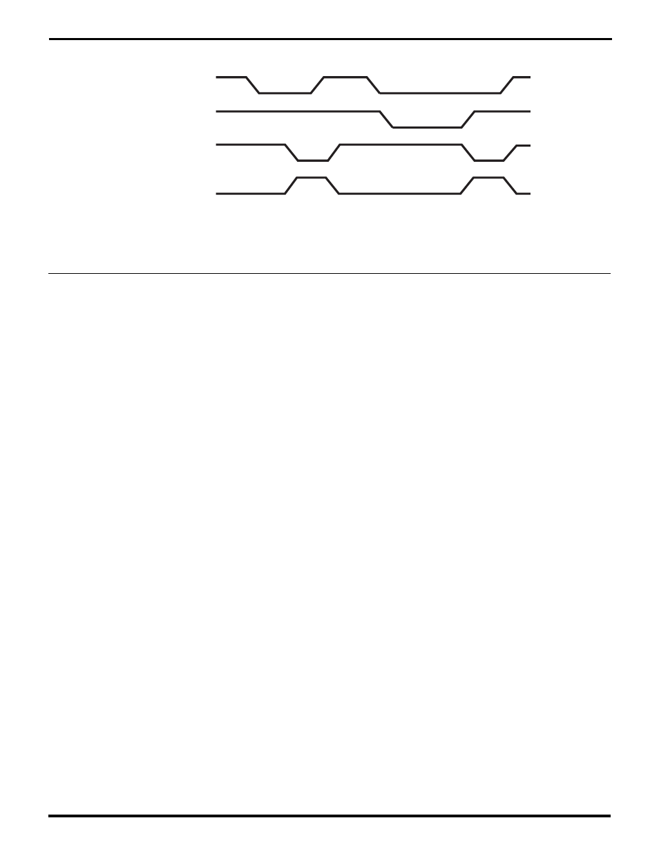
Figure 2-6. A Fast and Slow Cycle, with Three Kinds of Handshaking
2.6 PIN DESCRIPTIONS
/RESET.
Reset (input, active low). A low on this line places
the USC in a known, inactive state, and conditions it so that
the data, from the next write operation that asserts the /CS
pin, goes into the Bus Configuration Register (BCR) re-
gardless of register addressing. /RESET should be driven
low as soon as possible during power-up, and as needed
when restarting the overall system or the communications
subsystem.
AD15-AD0.
Address/Data Bus (inputs/tri-state outputs).
These lines carry data between the controlling micropro-
cessor and the USC, and may also carry multiplexed
addresses of registers within the USC. If the USC is used
with an external DMA controller, these lines also carry data
between the USC and system memory or the DMA control-
ler. AD15-AD0 can be used in a variety of ways based on
whether the USC senses activity on /AS after Reset, and on
the data written to the Bus Configuration Register (BCR).
/CS.
Chip Select (input, active low). A low on this line
indicates that the controlling microprocessor’s current bus
cycle refers to a register in the USC. The USC ignores /CS
when a low on /SITACK or /PITACK indicates that the
current bus operation is an interrupt acknowledge cycle.
On a multiplexed bus the USC latches the state of this pin
at rising edges on /AS, while on a non-multiplexed bus it
latches /CS at leading/falling edges on /DS, /RD, or /WR.
A//B.
Channel Select (input, high indicates “channel A”).
Cycles with /CS low, and /SITACK, /PITACK, and this pin
both high, access registers for channel A. Cycles with
/SITACK and /PITACK high, and /CS and this pin both low,
access registers for channel B. The state of this line when
the Bus Configuration Register is written determines “wait
vs. acknowledge” operation, as described later in this
chapter. On a multiplexed bus the USC latches the state
of this pin at rising edges on /AS, while on a non-multi-
plexed bus it latches the state at leading/falling edges on
/DS, /RD, or /WR.
D//C.
Data/Control (input, high indicates Data). A read
cycle with /CS low, and /SITACK, /PITACK, and this pin
high, fetches data from the receive FIFO of the channel
selected by A//B, via its Receive Data Register (RDR). A
write cycle with the same conditions writes data into that
channel’s transmit FIFO via its Transmit Data Register
(TDR). Cycles with /SITACK and /PITACK high and both
/CS and this pin low read or write a USC register. On a
multiplexed bus the USC determines which register to
access from the low-order AD lines at the rising edge of
/AS. On a non-multiplexed bus it typically selects the
register based on the LSBits of the serial controller’s
Channel Command/Address Register. On a multiplexed
bus the USC latches the state of this pin at rising edges on
/AS, while on a non-multiplexed bus it latches the state at
leading/falling edges on /DS, /RD, or /WR.
/AS.
Address Strobe (input, active low). After a reset, the
USC’s bus interface logic monitors this signal to see if the
host bus multiplexes address and data on AD15-AD0. If
the logic sees activity on /AS before (or as) software writes
the Bus Configuration Register, then in subsequent cycles
directed to the USC, it captures register selection from the
AD lines, A//B, and D//C on rising edges of /AS.
For a non-multiplexed bus this pin should be pulled up to
+5V. If a processor uses a non-multiplexed bus, yet has an
output called Address Strobe (e.g., 680x0 devices), this
pin should not be tied to the output.
UM009402-0201