Rainbow Electronics DS26519 User Manual
General description, Applications, Functional diagram
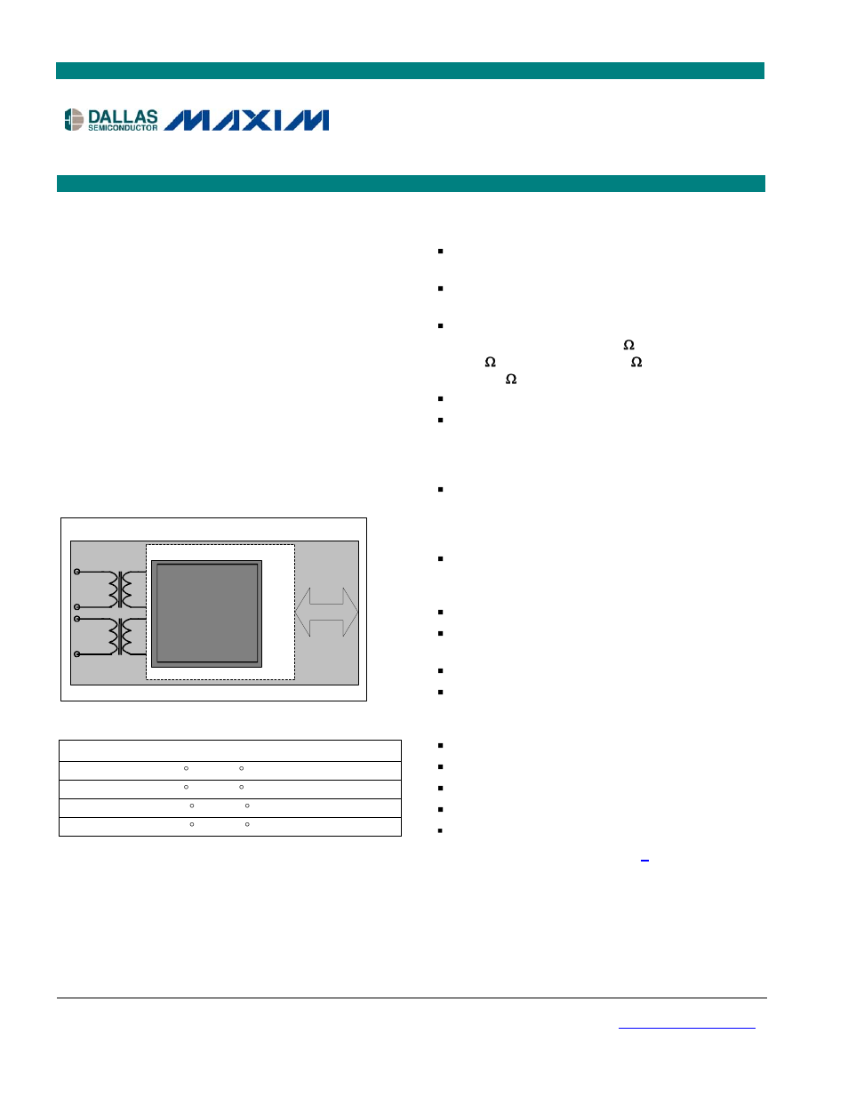
Table of contents
Document Outline
- TABLE OF CONTENTS
- 1. DETAILED DESCRIPTION
- 2. FEATURE HIGHLIGHTS
- 3. APPLICATIONS
- 4. SPECIFICATIONS COMPLIANCE
- 5. ACRONYMS AND GLOSSARY
- 6. MAJOR OPERATING MODES
- 7. BLOCK DIAGRAMS
- 8. PIN DESCRIPTIONS
- 9. FUNCTIONAL DESCRIPTION
- 9.1 Processor Interface
- 9.2 Clock Structure
- 9.3 Resets and Power-Down Modes
- 9.4 Initialization and Configuration
- 9.5 Global Resources
- 9.6 Per-Port Resources
- 9.7 Device Interrupts
- 9.8 System Backplane Interface
- 9.8.1 Elastic Stores
- 9.8.1.1 Elastic Stores Initialization
- 9.8.1.2 Minimum Delay Mode
- 9.8.1.3 Additional Receive Elastic Store Information
- 9.8.1.4 Receiving Mapped T1 Channels from a 2.048MHz Backplane
- 9.8.1.5 Mapping T1 Channels onto a 2.048MHz Backplane
- 9.8.1.6 Receiving Mapped E1 Transmit Channels from a 1.544MHz Backplane
- 9.8.1.7 Mapping E1 Channels onto a 1.544MHz Backplane
- 9.8.2 IBO Multiplexing
- 9.8.3 H.100 (CT Bus) Compatibility
- 9.8.4 Transmit and Receive Channel Blocking Registers
- 9.8.5 Transmit Fractional Support (Gapped Clock Mode)
- 9.8.6 Receive Fractional Support (Gapped Clock Mode)
- 9.8.1 Elastic Stores
- 9.9 Framers
- 9.9.1 T1 Framing
- 9.9.2 E1 Framing
- 9.9.3 T1 Transmit Synchronizer
- 9.9.4 Signaling
- 9.9.5 T1 Data Link
- 9.9.6 E1 Data Link
- 9.9.7 Maintenance and Alarms
- 9.9.8 Alarms
- 9.9.9 Error Count Registers
- 9.9.10 DS0 Monitoring Function
- 9.9.11 Transmit Per-Channel Idle Code Generation
- 9.9.12 Receive Per-Channel Idle Code Insertion
- 9.9.13 Per-Channel Loopback
- 9.9.14 E1 G.706 Intermediate CRC-4 Updating (E1 Mode Only)
- 9.9.15 T1 Programmable In-Band Loop Code Generator
- 9.9.16 T1 Programmable In-Band Loop Code Detection
- 9.9.17 Framer Payload Loopbacks
- 9.10 HDLC Controllers
- 9.11 Power-Supply Decoupling
- 9.12 Line Interface Units (LIUs)
- 9.13 Bit Error-Rate Test Function (BERT)
- 10. DEVICE REGISTERS
- 10.1 Register Listings
- 10.2 Register Bit Maps
- 10.3 Global Register Definitions
- 10.4 Framer Register Descriptions
- 10.4.1 Receive Register Descriptions
- Receive Idle Code Definition Registers 1 to 32
- Receive SLC96 Data Link Registers
- Received Sa7 Bits Register
- Received SaX Bits Register
- E1 Receive Digital Milliwatt Enable Registers 1 to 4
- Receive-Signaling Change of State Enable Registers 1 to 4
- RHPBA
- Receive-Signaling Reinsertion Enable Registers 1 to 4
- 0D4h, 0D5h, 0D6h, 0D7h + (200h x (n - 1)) + (2000h x [(n - 1) / 8]): where n = 1 to 16
- 10.4.2 Transmit Register Descriptions
- 10.4.1 Receive Register Descriptions
- 10.5 LIU Register Definitions
- 10.6 BERT Register Definitions
- 11. FUNCTIONAL TIMING
- 12. OPERATING PARAMETERS
- 13. AC TIMING CHARACTERISTICS
- 14. JTAG BOUNDARY SCAN AND TEST ACCESS PORT
- 15. PIN CONFIGURATION
- 16. PACKAGE INFORMATION
- 17. DOCUMENT REVISION HISTORY