Gfcr2 – Rainbow Electronics DS26519 User Manual
Page 134

DS26519 16-Port T1/E1/J1 Transceiver
134 of 310
Register Name:
GFCR2
Description:
Global Framer Control Register 2
Register Address:
20F1h
Channels:
9 to 16
Bit
#
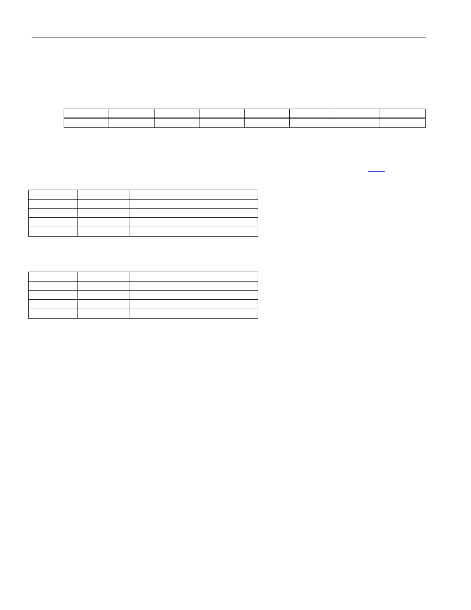
7 6 5 4 3 2 1 0
Name IBOMS1 IBOMS0 BPCLK1 BPCLK0
—
RFMSS TCBCS RCBCS
Default
0 0 0 0 0 0 0 0
Bits 7 and 6: Interleave Bus Operation Mode Select 1 and 0 (IBOMS[1:0]). These bits determine the
configuration of the IBO (interleaved bus) multiplexer and inform the framers of the IBO configuration. These bits
should be used in conjunction with the Rx and Tx IBO control registers within each of the framer units. These bits
control Channels 9 to 16. Additional information concerning the IBO multiplexer is given in Section
. These bits
must be set whether using the internal IBO mux or externally ganging the pins.
IBOMS1 IBOMS0
IBO
Mode
0 0
IBO
disabled.
0
1
2 devices on bus (4.096MHz).
1
0
4 devices on bus (8.192MHz).
1
1
8 devices on bus (16.384MHz).
Bits 5 and 4: Backplane Clock Select 1 and 0 (BPCLK[1:0]). These bits determine the clock frequency output on
the BPCLK2 pin.
BPCLK1 BPCLK0
BPCLK2
Frequency
0 0
2.048MHz
0 1
4.096MHz
1 0
8.192MHz
1 1
16.384MHz
Bit 2: Receive Frame/Multiframe Sync Select (RFMSS). This bit controls the function of all 16 RMSYNCn/
RFSYNCn pins.
0 = RMSYNC/RFSYNC[16:9] pins output RFSYNC[16:9] (Receive Frame Sync)
1 = RMSYNC/RFSYNC[16:9] pins output RMSYNC[16:9] (Receive Multiframe Sync)
Bit 1: Transmit Channel Block/Clock Select (TCBCS). This bit controls the function of all 16 TCHBLKn/
TCHCLKn pins.
0 = TCHBLK/TCHCLK[16:9] pins output TCHBLK[16:9] (Transmit Channel Block)
1 = TCHBLK/TCHCLK[16:9] pins output TCHCLK[16:9] (Transmit Channel Clock)
Bit 0: Receive Channel Block/Clock Select (RCBCS). This bit controls the function of all 16 RCHBLKn/
RCHCLKn pins.
0 = RCHBLK/RCHCLK[16:9] pins output RCHBLK[16:9] (Receive Channel Block)
1 = RCHBLK/RCHCLK[16:9] pins output RCHCLK[16:9] (Receive Channel Clock)
