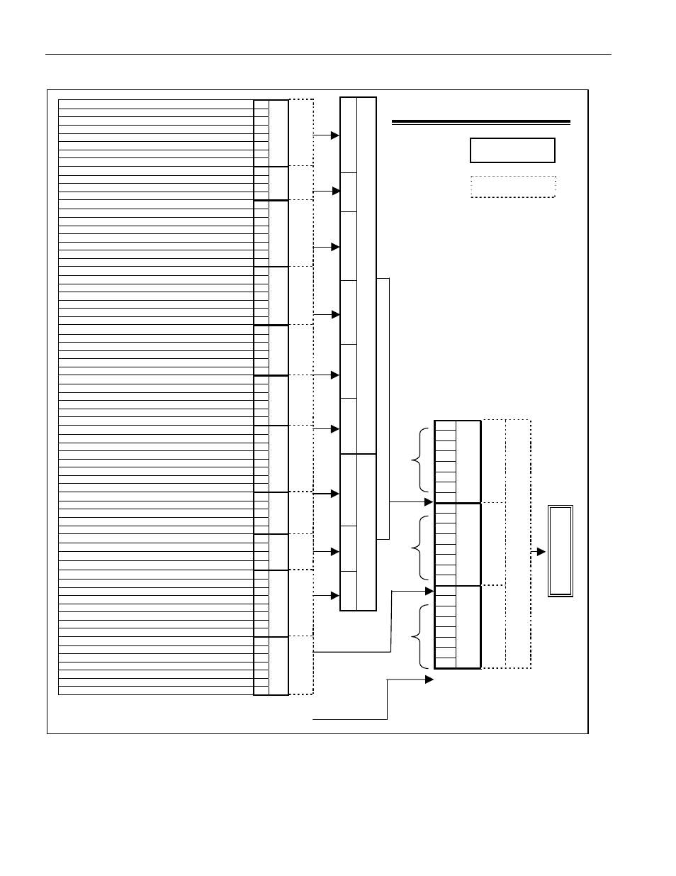
Figure 9-11, Interrup t pin, Gfisr1 gfimr1 – Rainbow Electronics DS26519 User Manual
Page 42: Glisr1 glimr1, Gbisr1 gbimr1

DS26519 16-Port T1/E1/J1 Transceiver
42 of 310
Figure 9-11. Device Interrupt Information Flow Diagram
Receive Remote Alarm Indication Clear
7
Receive Alarm Condition Clear
6
Receive Loss of Signal Clear
5
Receive Loss of Frame Clear
4
Receive Remote Alarm Indication
3
Receive Alarm Condition
2
Receive Loss of Signal
1
Receive Loss of Frame
0
RL
S1
RIM
1
Receive Signal All Ones
3
Receive Signal All Zeros
2
Receive CRC4 Multiframe
1
Receive Align Frame
0
RL
S
2
RIM
2
Loss of Receive Clk Clear / Loss of Receive Clk Clear
7
Spare Code Detected Condition Clear / -
6
Loop Down Code Clear / V52 Link Clear
5
Loop Up Code Clear / Receive Distant MF Alarm Clear
4
Loss of Receive Clk / Loss of Receive Clk
3
Spare Code Detect / -
2
Loop Down Detect / V52 Link Detect
1
Loop Up Detect / Receive Distant MF Alarm Detect
0
RL
S3
RIM
3
Receive Elastic Store Full
7
Receive Elastic Store Empty
6
Receive Elastic Store Slip
5
Receive Signaling Change of State (Enable in RSCSE1-4) 3
One Second Timer
2
Timer 1
Receive Multiframe
0
RL
S4
RIM
4
Receive FIFO Overrun
5
Receive HDLC Opening Byte
4
Receive Packet End
3
Receive Packet Start
2
Receive Packet High Watermark
1
Receive FIFO Not Empty
0
RL
S5
RIM
5
Receive RAI-CI
5
Receive AIS-CI
4
Receive SLC-96 Alignment
3
Receive FDL Register Full
2
Receive BOC Clear
1
Receive BOC
0
RL
S7
RIM
7
Transmit Elastic Store Full
7
Transmit Elastic Store Empty
6
Transmit Elastic Store Slip
5
Transmit SLC96 Multiframe
4
Transmit Align Frame
3
Transmit Multiframe
2
Loss of Transmit Clock Clear
1
Loss of Transmit Clock
0
TLS1
TI
M1
Transmit FDL Register Empty
4
Transmit FIFO Underrun
3
Transmit Message End
2
Transmit FIFO Below Low Watermark
1
Transmit FIFO Not Full Set
0
TLS2
TI
M2
- -
- -
Loss of Frame
1
Loss of Frame Synchronization
0
TLS3
TI
M3
Jitter Attenuator Limit Trip Clear
7
Open Circuit Detect Clear
6
Short Circuit Detect Clear
5
Loss of Signal Detect Clear
4
Jitter Attenuator Limit Trip
3
Open Circuit Detect
2
Short Circuit Detect
1
Loss of Signal Detect
0
LLSR
LSI
M
R
BERT Bit Error Detected
6
BERT Bit Counter Overflow
5
BERT Error Counter Overflow
4
BERT Receive All Ones
3
BERT Receive All Zeros
2
BERT Receive Loss of Synchronization
1
BERT in Synchronization
0
BL
SR
BS
IM
Interrup
t Pin
0
1
2
3
4
5
RIIR
2
1
0
TIIR
7
6
5
4
3
2
1
0
GFISR1
GFIMR1
7
6
5
4
3
2
1
0
GLISR1
GLIMR1
7
6
5
4
3
2
1
0
GBISR1
GBIMR1
GTC
R
1.0
Framers 2
-8
LIUs 2-8
BERT
s 2-8
Drawing Legend:
Interrupt Status
Registers
Register Name
Interrupt Mask
Registers
Register Name
