Tcbr1, Thscs1, Funct – Rainbow Electronics DS26519 User Manual
Page 247: Rscse4, Tcbr2, Tcbr3, Tcbr4, Thscs2, Thscs3, Thscs4
DS26519 16-Port T1/E1/J1 Transceiver
247 of 310
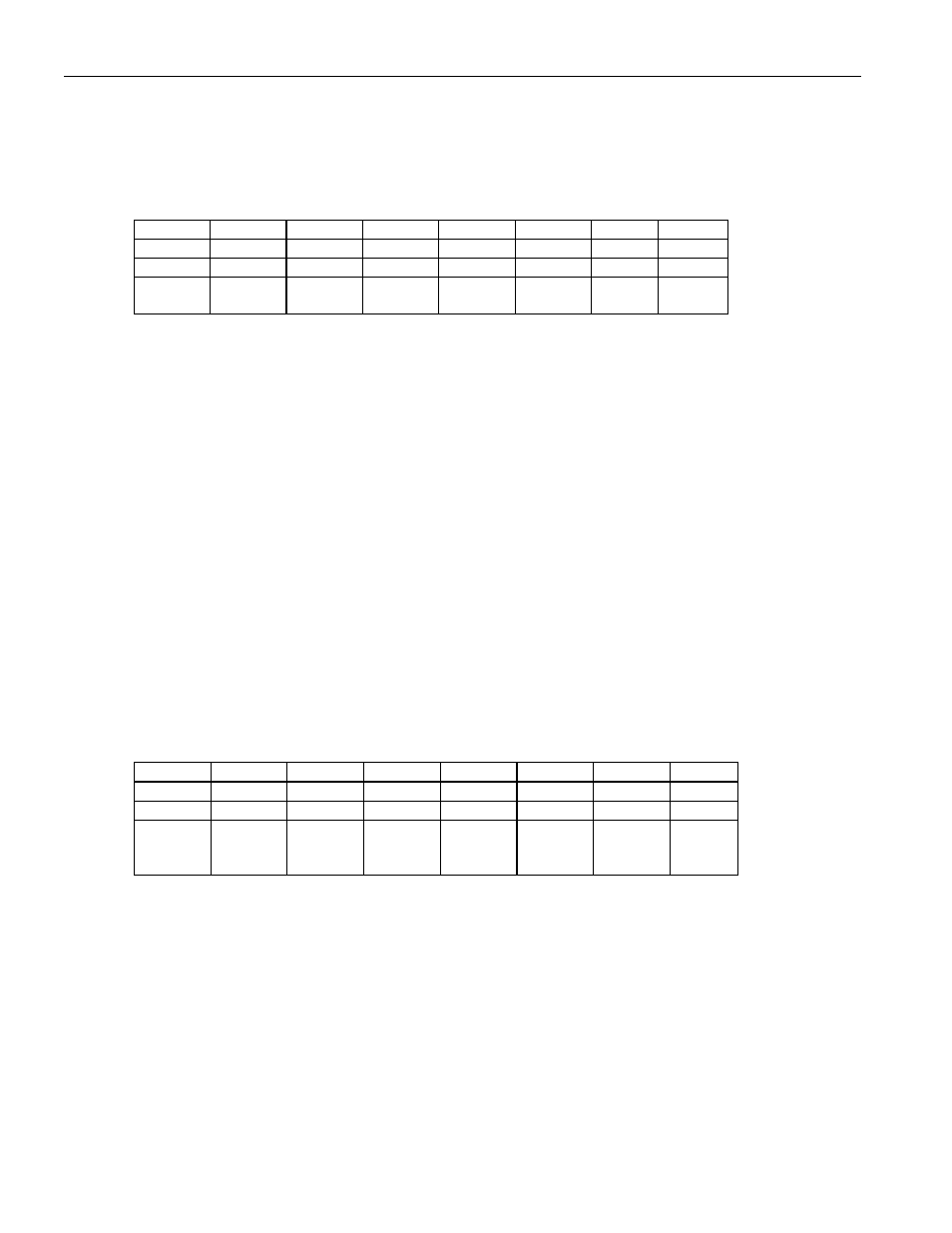
Register Name:
TCBR1, TCBR2, TCBR3, TCBR4
Register Description:
Transmit Channel Blocking Registers 1 to 4
Register Address:
1C4h, 1C5h, 1C6h, 1C7h + (200h x (n - 1)) + (2000h x [(n - 1) / 8]): where n = 1 to 16
(MSB)
(LSB)
Bit
# 7 6 5 4 3 2 1
0
Name CH8 CH7 CH6 CH5 CH4 CH3 CH2
CH1
TCBR1
CH16 CH15 CH14 CH13 CH12 CH11 CH10 CH9
TCBR2
CH24 CH23 CH22 CH21 CH20 CH19 CH18
CH17
TCBR3
CH32 CH31 CH30 CH29 CH28 CH27 CH26
CH25
(F-bit)
TCBR4 (E1
Mode Only)*
Bits 7 to 0: Transmit Channels 1 to 32 Channel Blocking Control Bits (CH[1:32]).
0 = Force the TCHBLKn pin to remain low during this channel time.
1 = Force the TCHBLKn pin high during this channel time.
* Note that TCBR4 has two functions:
When 2.048MHz backplane mode is selected, this register allows the user to enable the channel blocking
signal for any of the 32 possible backplane channels.
When 1.544MHz backplane mode is selected, the LSB of this register determines whether or not the
TCHBLKn signal will pulse high during the F-bit time:
TCBR4.0 = 0, do not pulse TCHBLKn during the F-bit.
TCBR4.0 = 1, pulse TCHBLKn during the F-bit.
In this mode TCBR4.1 to TCBR4.7 should be set to 0.
Register Name:
THSCS1, THSCS2, THSCS3, THSCS4
Register Description:
Transmit Hardware-Signaling Channel Select Registers 1 to 4
Register Address:
1C8h, 1C9h, 1CAh, 1CBh + (200h x (n - 1)) + (2000h x [(n - 1) / 8]): where n = 1 to 16
(MSB)
(LSB)
Bit
# 7 6 5 4 3 2 1 0
Name CH8 CH7 CH6 CH5 CH4 CH3 CH2 CH1
THSCS1
CH16 CH15 CH14 CH13 CH12 CH11 CH10 CH9
THSCS2
CH24 CH23 CH22 CH21 CH20 CH19 CH18 CH17
THSCS3
CH32 CH31 CH30 CH29 CH28 CH27 CH26 CH25
THSCS4
(E1 Mode
Only)*
Bits 7 to 0: Transmit Hardware-Signaling Channel Select for Channels 1 to 32 (CH[1:32]). These bits
determine which channels have signaling data inserted from the TSIGn pin into the TSERn PCM data.
0 = Do not source signaling data from the TSIGn pin for this channel.
1 = Source signaling data from the TSIGn pin for this channel.
* Note that THSCS4 is only used in 2.048MHz backplane applications.