Common characteristics, Sram read cycle, Sram write cycle – Epson S1C33210 User Manual
Page 90
8 ELECTRICAL CHARACTERISTICS
A-76
EPSON
S1C33210 PRODUCT PART
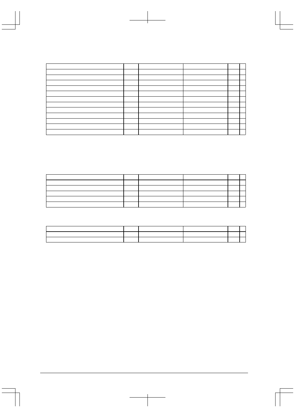
Common characteristics
(Unless otherwise specified: V
DD
=2.7V to 3.6V, V
SS
=0V, Ta=-40
°
C to +85
°
C)
Item
Symbol
Min.
Max.
Unit
∗
Address delay time
t
AD
–
10
ns
1
#CEx delay time (1)
t
CE1
–
10
ns
#CEx delay time (2)
t
CE2
–
10
ns
Wait setup time
t
WTS
17
–
ns
Wait hold time
t
WTH
0
–
ns
Read signal delay time (1)
t
RDD1
10
ns
2
Read data setup time
t
RDS
15
ns
Read data hold time
t
RDH
0
ns
Write signal delay time (1)
t
WRD1
10
ns
3
Write data delay time (1)
t
WDD1
10
ns
Write data delay time (2)
t
WDD2
0
10
ns
Write data hold time
t
WDH
0
ns
∗
note 1) This applies to the #BSH and #BSL timings.
2) This applies to the #GAAS and #GARD timings.
3) This applies to the #GAAS timing.
SRAM read cycle
(Unless otherwise specified: V
DD
=2.7V to 3.6V, V
SS
=0V, Ta=-40
°
C to +85
°
C)
Item
Symbol
Min.
Max.
Unit
∗
Read signal delay time (2)
t
RDD2
10
ns
Read signal pulse width
t
RDW
t
CYC
(0.5+WC)-10
ns
Read address access time (1)
t
ACC1
t
CYC
(1+WC)-25
ns
Chip enable access time (1)
t
CEAC1
t
CYC
(1+WC)-25
ns
Read signal access time (1)
t
RDAC1
t
CYC
(0.5+WC)-25
ns
SRAM write cycle
(Unless otherwise specified: V
DD
=2.7V to 3.6V, V
SS
=0V, Ta=-40
°
C to +85
°
C)
Item
Symbol
Min.
Max.
Unit
∗
Write signal delay time (2)
t
WRD2
10
ns
Write signal pulse width
t
WRW
t
CYC
(1+WC)-10
ns