I/o memory of input ports, Or "0" when the voltage is low (v – Epson S1C33210 User Manual
Page 365

III PERIPHERAL BLOCK: INPUT/OUTPUT PORTS
S1C33210 FUNCTION PART
EPSON
B-III-9-3
I/O Memory of Input Ports
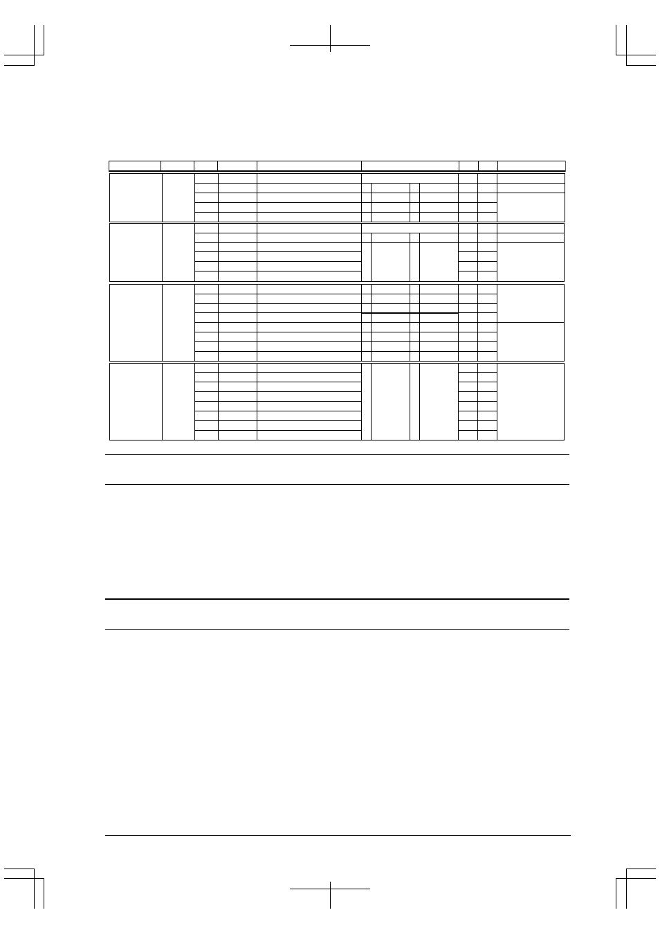
Table 9.2 shows the control bits of the input ports.
Table 9.2 Control Bits of Input Ports
Name
Address
Register name
Bit
Function
Setting
Init.
R/W
Remarks
–
CP4
CFK52
CFK51
CFK50
D7–4
D3
D2
D1
D0
reserved
CP4
K52 function selection
K51 function selection
K50 function selection
–
–
0
0
0
0
–
R/W
R/W
R/W
R/W
Undefined when read.
Always set to 0.
00402C0
(B)
1 –
0 CP4
1 #ADTRG
0 K52
1 #DMAREQ1 0 K51
1 #DMAREQ0 0 K50
K5 function
select register
–
–
CP4D
K52D
K51D
K50D
D7–5
D4
D3
D2
D1
D0
reserved
–
CP4 data
K52 input port data
K51 input port data
K50 input port data
–
–
–
–
–
–
–
–
R
R
R
R
R
0 when being read.
Undefined when read.
00402C1
(B)
1
1
–
High
0
0
–
Low
K5 input port
data register
CP3
CP2
CP1
CP0
CFK63
CFK62
CFK61
CFK60
D7
D6
D5
D4
D3
D2
D1
D0
CP3
CP2
CP1
CP0
K63 function selection
K62 function selection
K61 function selection
K60 function selection
0
0
0
0
0
0
0
0
R/W
R/W
R/W
R/W
R/W
R/W
R/W
R/W
Always set to 0.
00402C3
(B)
1 –
0 CP3
1 –
0 CP2
1 –
0 CP1
1 –
0 CP0
1 AD3
0 K63
1 AD2
0 K62
1 AD1
0 K61
1 AD0
0 K60
K6 function
select register
CP3D
CP2D
CP1D
CP0D
K63D
K62D
K61D
K60D
D7
D6
D5
D4
D3
D2
D1
D0
CP3 data
CP2 data
CP1 data
CP0 data
K63 input port data
K62 input port data
K61 input port data
K60 input port data
–
–
–
–
–
–
–
–
R
R
R
R
R
R
R
R
00402C4
(B)
1 High
0 Low
K6 input port
data register
CFK52–CFK50: K5[2:0] function selection (D[2:0]) / K5 function select register (0x402C0)
CFK63–CFK60: K6[3:0] function selection (D[3:0]) / K6 function select register (0x402C3)
Selects the function of each input-port pin.
Write "1": Used for peripheral circuit
Write "0": Input port pin
Read: Invalid
When a bit of the CFK register is set to "1", the corresponding pin is set for use with the peripheral circuit (see Table
9.1). The pins for which register bits are set to "0" can be used as general-purpose input ports.
At cold start, CFK is set to "0" (input port). At hot start, CFK retains its state from prior to the initial reset.
K52D–K50D: K5[2:0] input port data (D[2:0]) / K5 input port data register (0x402C1)
K63D–K60D: K6[3:0] input port data (D[3:0]) / K6 input port data register (0x402C4)
The input data on each input port pin can be read from this register.
Read "1": High level
Read "0": Low level
Write: Invalid
The pin voltage of each input port can be read out "1" directly when the voltage is high (V
DD
) or "0" when the voltage
is low (V
SS
) respectively.
Since this register is a read-only register, writing to the register is ignored.
When the ports set for A/D converter input are read, the value obtained is always "0".
