Epson S1C33210 User Manual
Page 23
1 OUTLINE
S1C33210 PRODUCT PART
EPSON
A-9
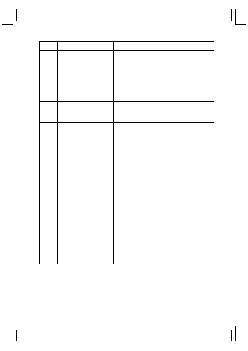
Pin name
Pin No.
I/O
Pull-up
Function
QFP15-128
P13
EXCL3
T8UF3
DPCO
124
I/O
–
P13:
I/O port when CFP13(D3/0x402D4) = "0" and
CFEX1(D1/0x402DF) = "0"
EXCL3:
16-bit timer 3 event counter input when CFP13(D3/0x402D4) =
"1", IOC13(D3/0x402D6) = "0" and CFEX1(D1/0x402DF) = "0"
T8UF3:
8-bit timer 3 output when CFP13(D3/0x402D4) = "1",
IOC13(D3/0x402D6) = "1" and CFEX1(D1/0x402DF) = "0"
DPCO:
DPCO signal output when CFEX1(D1/0x402DF) = "1" (default)
P14
FOSC1
DCLK
125
I/O
–
P14:
I/O port when CFP14(D4/0x402D4) = "0" and
CFEX0(D0/0x402DF) = "0"
FOSC1:
OSC1 clock output when CFP14(D4/0x402D4) = "1" and
CFEX0(D0/0x402DF) = "0"
DCLK:
DCLK signal output when CFEX0(D0/0x402DF) = "1" (default)
P15
EXCL4
#DMAEND0
128
I/O
–
P15:
I/O port when CFP15(D5/0x402D4) = "0" (default)
EXCL4:
16-bit timer 4 event counter input when CFP15(D5/0x402D4) =
"1" and IOC15(D5/0x402D6) = "0"
#DMAEND0: HSDMA Ch. 0 end-of-transfer signal output when
CFP15(D5/0x402D4) = "1" and IOC15(D5/0x402D6) = "1"
P16
EXCL5
#DMAEND1
77
I/O
–
P16:
I/O port when CFP16(D6/0x402D4) = "0" (default)
EXCL5:
16-bit timer 5 event counter input when CFP16(D6/0x402D4) =
"1" and IOC16(D6/0x402D6) = "0"
#DMAEND1: HSDMA Ch. 1 end-of-transfer signal output when
CFP16(D6/0x402D4) = "1" and IOC16(D6/0x402D6) = "1"
P20
#DRD
92
I/O
–
P20:
I/O port when CFP20(D0/0x402D8) = "0" (default)
#DRD:
DRAM read signal output for successive RAS mode when
CFP20(D0/0x402D8) = "1"
P21
#DWE
#GAAS
117
I/O
–
P21: I/O
port
when
CFP21(D1/0x402D8)
=
"0"
and
CFEX2(D2/0x402DF) = "0" (default)
#DWE: DRAM
read
signal
output
for
successive
RAS
mode
when
CFP21(D1/0x402D8) = "1" and CFEX2(D2/0x402DF) = "0"
#GAAS: Area
address
strobe
for
GA
when
CFEX2(D2/0x402DF)
=
"1"
P22
TM0
118
I/O
–
P22:
I/O port when CFP22(D2/0x402D8) = "0" (default)
TM0:
16-bit timer 0 output when CFP22(D2/0x402D8) = "1"
P23
TM1
119
I/O
–
P23:
I/O port when CFP23(D3/0x402D8) = "0" (default)
TM1:
16-bit timer 1 output when CFP23(D3/0x402D8) = "1"
P24
TM2
#SRDY2
126
I/O
–
P24:
I/O port when CFP24(D4/0x402D8) = "0" (default)
TM2:
16-bit timer 2 output when CFP24(D4/0x402D8) = "1"
#SRDY2:
Serial I/F Ch.2 ready signal input/output when
SSRDY2(D3/0x402DB) = "1" and CFP24 (D4/0x402D8) = "0"
P25
TM3
#SCLK2
127
I/O
–
P25:
I/O port when CFP25(D5/0x402D8) = "0" (default)
TM3:
16-bit timer 3 output when CFP25(D5/0x402D8) = "1"
#SCLK2:
Serial I/F Ch.2 clock input/output when SSCLK2(D2/0x402DB) =
"1" and CFP25(D5/0x402D8) = "0"
P26
TM4
SOUT2
1
I/O
–
P26:
I/O port when CFP26(D6/0x402D8) = "0" (default)
TM4:
16-bit timer 4 output when CFP26(D6/0x402D8) = "1"
SOUT2:
Serial I/F Ch.2 data output when SSOUT2(D1/0x402DB) = "1"
and CFP26(D6/0x402D8) = "0"
P27
TM5
SIN2
2
I/O
–
P27:
I/O port when CFP27(D7/0x402D8) = "0" (default)
TM5:
16-bit timer 5 output when CFP27(D7/0x402D8) = "1"
SIN2:
Serial I/F Ch.2 data input when SSIN2(D0/0x402DB) = "1" and
CFP27(D7/0x402D8) = "0"