Crc checking, Output port control, Input port monitoring – Epson S1C33210 User Manual
Page 395
III PERIPHERAL BLOCK: MONITORED MOBILE ACCESS INTERFACES
S1C33210 FUNCTION PART
EPSON
B-III-10-9
bit 7
¥¥¥¥¥¥¥¥¥¥¥¥¥¥¥¥¥¥¥¥
0x0200580
0x020057E
0x0200540
0x020053E
0x0200500
0x02004FE
0x0200480
0x020047E
0x0200440
0x020043E
0x0200400
Receive Buffer B
(32 bytes)
Receive Buffer A
(32 bytes)
Transmit Buffer B
(32 bytes)
Transmit Buffer A
(32 bytes)
Figure 10.8 PDC Communications Mode Data Buffers
CRC Checking
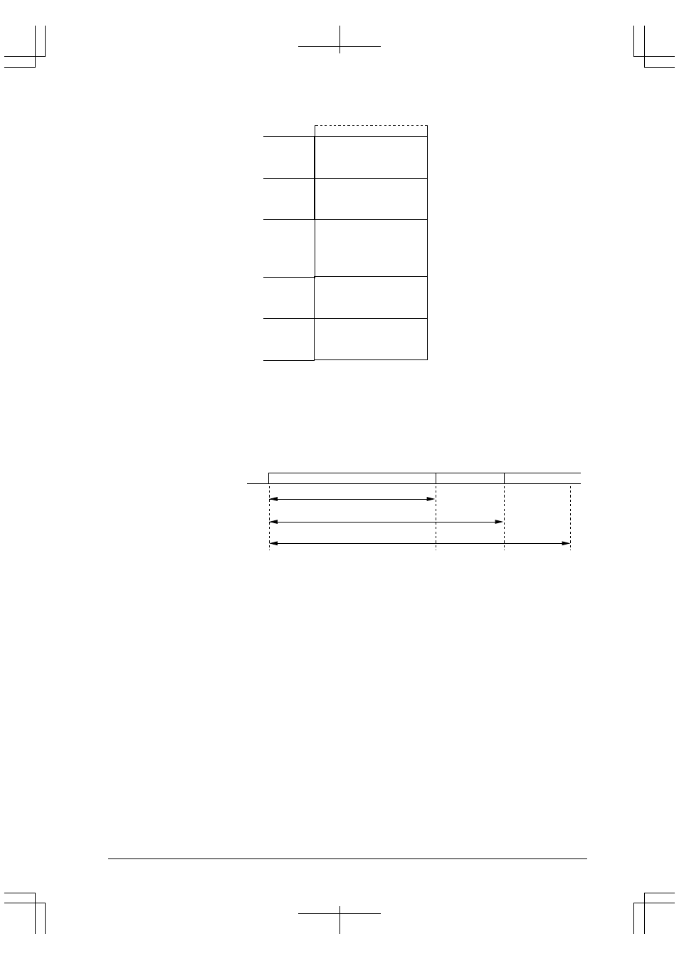
PDC communications uses the following two CRC polynomials for validating frame data integrity. Figure 10.9
shows the ranges of application for each one.
CRC-16
: G(
χ
) =
χ
16
+
χ
15
+
χ
2
+ 1
CRC-CCITT
: G(
χ
) =
χ
16
+
χ
12
+
χ
5
+ 1
Serial data
Input for CRC-16 calculation (192 bits)
Input for CRC-CCITT calculation (208 bits)
Frame data (224 bits)
Serial data (192 bits)
CRC-16 (16 bit)
CRC-CCITT (16 bit)
Figure 10.9 PDC Communications Mode
Output Port Control
For communications macro select (MCRS) register (D[1:0]/0x200000) settings other than 00–that is, HDLC,
PDC, and PHS communications modes–the MOPORT3 and MOPORT2 bits in the communications block
output port data register (D[3:0]/0x020000A) drive the RTS and DTR pins using negative logic.
Input Port Monitoring
The MIPORT[1:0] bits in the communications block input port data register (D[1:0]/0x020000C) track the
input levels for the DSR and RI pins. Note that the block does not store these values internally.
In this mode as in others, setting the GOUTE bit in the communications block input port data register
(D7/0x020000C) to "1" connects the RI input to the GOUT output pin.
Note: Bits in the communications block modem status register (0x020002A) also track the input levels for
the DSR and RI pins as well as transitions for triggering interrupt requests with changes in pin
states.