I/o control register and i/o modes – Epson S1C33210 User Manual
Page 367
III PERIPHERAL BLOCK: INPUT/OUTPUT PORTS
S1C33210 FUNCTION PART
EPSON
B-III-9-5
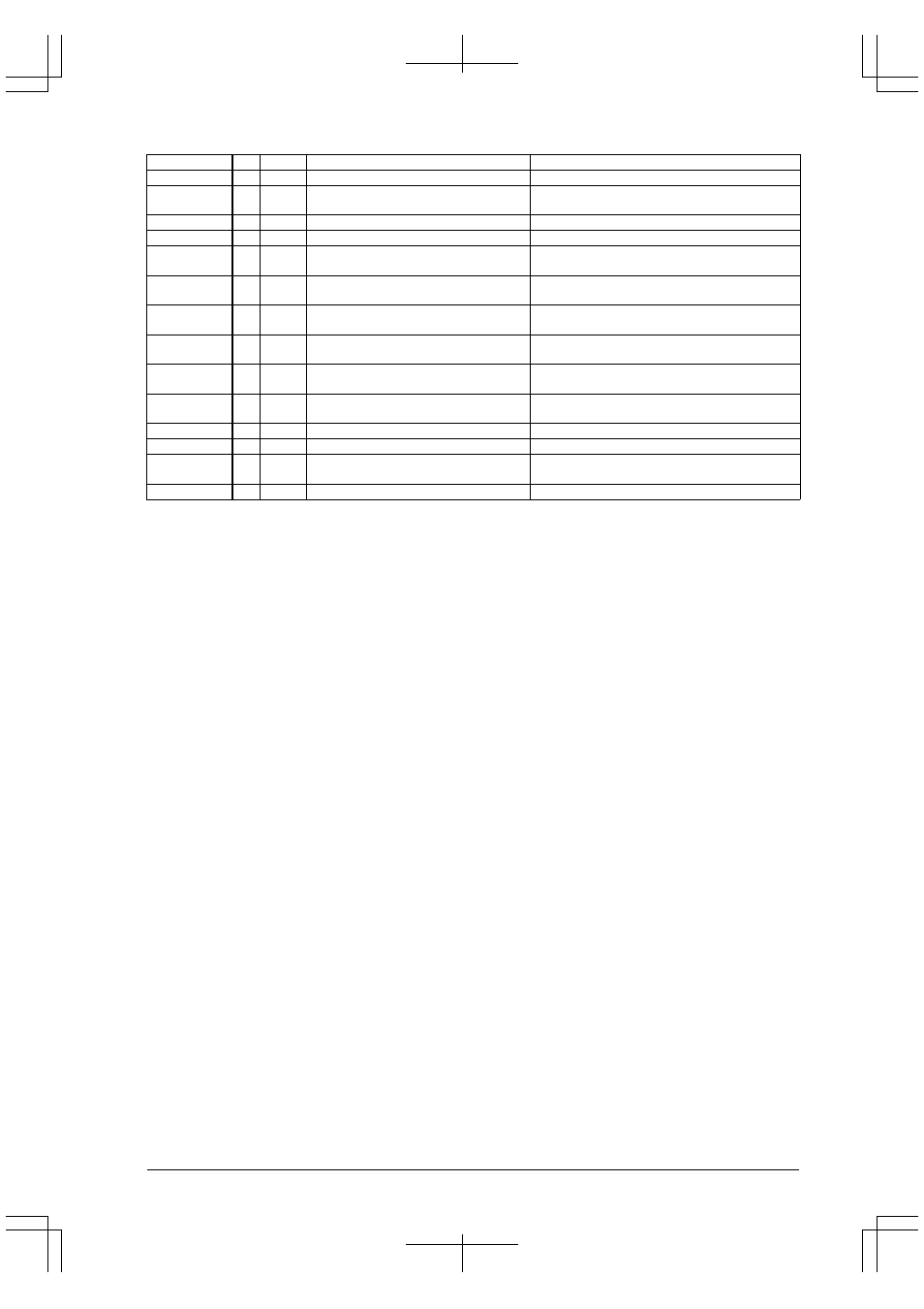
Pin name
I/O
Pull-up
Function
Function select bit
P20/#DRD
I/O
–
I/O port / #DRD output
CFP20(D0)/P2 function select register(0x402D8)
P21/#DWE/
#GAAS
I/O
–
I/O port / #DWE output /
GA address strobe output (Ex)
CFP21(D1)/P2 function select register(0x402D8)
CFEX2(D2)/Port function extension register(0x402DF)
P22/TM0
I/O
–
I/O port / 16-bit timer 0 output
CFP22(D2)/P2 function select register(0x402D8)
P23/TM1
I/O
–
I/O port / 16-bit timer 1 output
CFP23(D3)/P2 function select register(0x402D8)
P24/TM2/
#SRDY2
I/O
–
I/O port / 16-bit timer 2 output / Serial IF Ch.2
ready input/output
CFP24(D4)/P2 function select register(0x402D8)
P25/TM3/
#SCLK2
I/O
–
I/O port / 16-bit timer 3 output / Serial IF Ch.2
clock input/output
CFP25(D5)/P2 function select register(0x402D8)
P26/TM4/
SOUT2
I/O
–
I/O port / 16-bit timer 4 output / Serial IF Ch.2
data output
CFP26(D6)/P2 function select register(0x402D8)
P27/TM5/SIN2
I/O
–
I/O port / 16-bit timer 5 output / Serial IF Ch.2
data input
CFP27(D7)/P2 function select register(0x402D8)
P30/#WAIT/
#CE4&5
I/O
–
I/O port / #WAIT input (I) / #CE4&5 output (O) CFP30(D0)/P3 function select register(0x402DC)
P31/#BUSGET/
#GARD
I/O
–
I/O port / #BUSGET output /
GA read signal output (Ex)
CFP31(D1)/P3 function select register(0x402DC)
CFEX3(D3)/Port function extension register(0x402DF)
P32/#DMAACK0 I/O
–
I/O port / #DMAACK0 output
CFP32(D2)/P3 function select register(0x402DC)
P33/#DMAACK1 I/O
–
I/O port / #DMAACK1 output
CFP33(D3)/P3 function select register(0x402DC)
P34/#BUSREQ/
#CE6
I/O
–
I/O port / #BUSREQ input (I) / #CE6 output (O) CFP34(D4)/P3 function select register(0x402DC)
P35/#BUSACK
I/O
–
I/O port / #BUSACK output
CFP35(D5)/P3 function select register(0x402DC)
(I): Input mode, (O): Output mode, (Ex): Extended function
At cold start, all pins are set for I/O ports Pxx (function select register CFPxx = "0"). When these pins are used for
the internal peripheral circuits, write "1" to CFPxx. For details on pin functions in this case, refer to the description of
each peripheral circuit in this manual.
At hot start, the pins retain their state from prior to the reset.
In addition to being an I/O port, the P10–P13, P15–P16, P30 and P34 pins are shared with two types (three types for
P10–P13) of peripheral circuits. The type of peripheral circuit for which these pins are used is determined by the
direction (input or output) in which the pin is set using an I/O control register, as will be described later.
The P04–P05, P10–P14, P21 and P31 ports have extended functions indicated with (Ex) in the table. They can be
selected by writing "1" to CFEXx / Port function extension register (0x402DF).
The setting of CFEXx has priority over the CFPxx.
At cold start, CFEX1 and CFEX0 are set to "1", so the P10–P14 pins are set for debug signal outputs.
I/O Control Register and I/O Modes
The I/O ports are directed for input or output modes by writing data to an I/O control register corresponding to each
port bit.
P05–P00 I/O control: IOC0[5:0] (D[5:0]) / P0 I/O control register (0x402D2)
P16–P10 I/O control: IOC1[6:0] (D[6:0]) / P1 I/O control register (0x402D6)
P27–P20 I/O control: IOC2[7:0] (D[7:0]) / P2 I/O control register (0x402DA)
P35–P30 I/O control: IOC3[5:0] (D[5:0]) / P3 I/O control register (0x402DE)
To set an I/O port for input, write "0" to the I/O control bit. I/O ports set for input mode are placed in the high-
impedance state, and thus function as input ports.
In the input mode, the state of the input pin is read directly, so the data is "1" when the pin state is high (V
DD
level) or
"0" when the pin state is low (V
SS
level).
Even in the input mode, data can be written to the data register without affecting the pin state.
To set an I/O port for output, write "1" to the I/O control bit. I/O port set for output function as output ports. When the
port output data is "1", the port outputs a high level (V
DD
level); when the data is "0", the port outputs a low level
(V
SS
level).
At cold start, the I/O control register is set to "0" (input mode).
At hot start, the pins retain their state from prior to the reset.
Note: If pins P10–P14, P15–P16, P30 and P34 are set for use with peripheral circuits, their pin functions
vary depending on the input/output direction control by the IOC1x register.