Dram direct interface, Outline of dram interface – Epson S1C33210 User Manual
Page 175

II CORE BLOCK: BCU (Bus Control Unit)
S1C33210 FUNCTION PART
EPSON
B-II-4-23
DRAM Direct Interface
Outline of DRAM Interface
The BCU incorporates a DRAM direct interface that allows DRAM to be connected directly to areas 8 and 7 or areas
14 and 13. This interface supports the 2CAS method, so that column addresses can be set at between 8 and 11 bits. In
addition, this interface supports a fast-page or an EDO-page mode (EDO DRAM directly connectable to areas) as
well as random cycles. The refresh method (CAS-before-RAS refresh or self-refresh) and timing conditions (e.g.,
number of RAS/CAS cycles and number of precharge cycles) can be programmed using a control bit.
When selecting areas 8 and 7 or areas 14 and 13 to be used for DRAM, it depends on chip-enable settings using
CEFUNC (D9) / DRAM timing set-up register (0x48130).
CEFUNC = "00": DRAM can be connected to areas 8 and 7 (default)
#CE8 and #CE7 function as #RAS0 and #RAS1, respectively.
CEFUNC
≠
"00": DRAM can be connected to areas 14 and 13.
#CE14 and #CE13 function as #RAS2 and #RAS3, respectively.
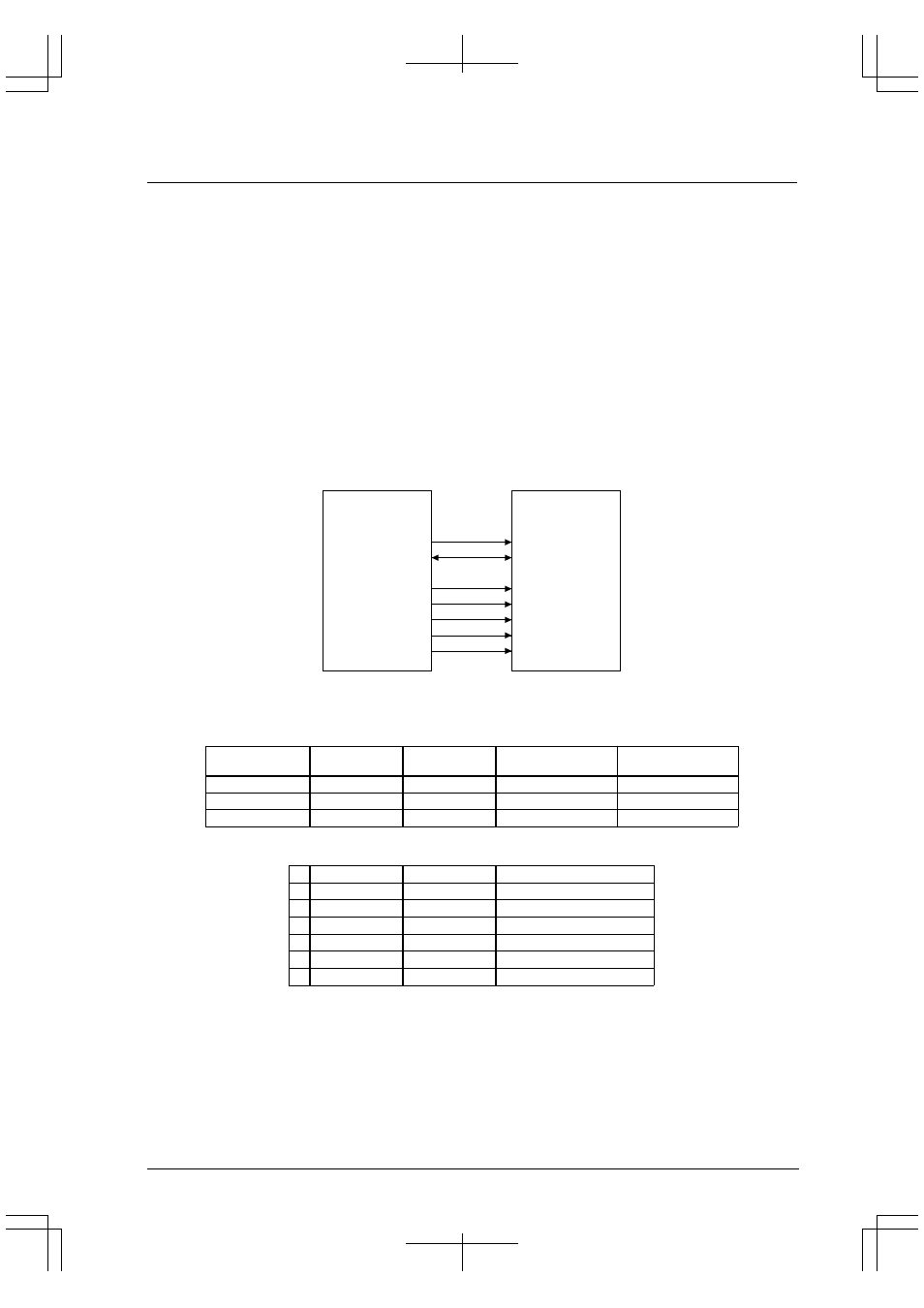
Figure 4.27 shows a sample DRAM connection. Table 4.13 and Table 4.14 show examples of connectable DRAMs
and typical configurations.
A[9:1]
D[15:0]
#RD
#RASx(#CEx)
*
#HCAS
#LCAS
#WE
S1C33
A[8:0]
I/O[15:0]
#OE
#RAS
#HCAS
#LCAS
#WE
4M DRAM
(256K x 16)
∗
x: 14, 13, 8 or 7
Figure 4.27 Sample DRAM Connection
Table 4.13 Connectable DRAM Example
DRAM
Number of
devices
Number of
Row bits
Number of
Column bits
Memory size
1M (64K x 16)
1
8
8
128K bytes
4M (256K x 16)
1
9
9
512K bytes
16M (1M x 16)
1
12
8
2M bytes
Table 4.14 DRAM Configuration Example (areas 7 and 8 only)
Area 7
Area 8
Total memory size
1 I/O
DRAM (1M)
1M bits
(128K bytes)
2 I/O
DRAM (4M)
4M bits
(512K bytes)
3 I/O
DRAM (16M)
16M bits
(2M bytes)
4 DRAM (1M)
DRAM (1M)
2M bits
(256K bytes)
5 DRAM (4M)
DRAM (4M)
8M bits
(1M bytes)
6 DRAM (16M)
DRAM (16M)
32M bits
(4M bytes)
