Epson S1C33210 User Manual
Page 165
II CORE BLOCK: BCU (Bus Control Unit)
S1C33210 FUNCTION PART
EPSON
B-II-4-13
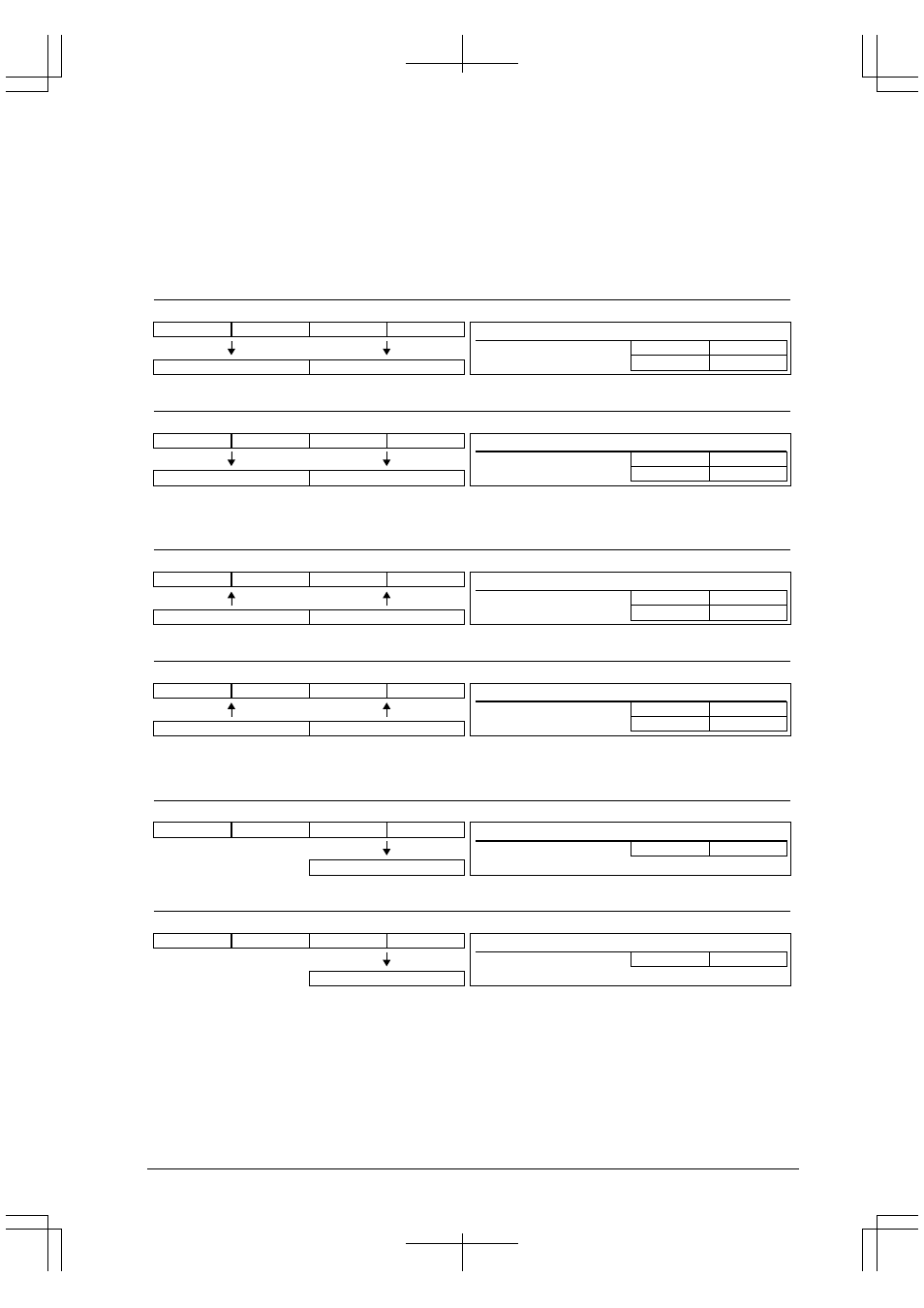
These bus operations are shown in the figure below, taking the example of the A0 method.
With the BSL method, the following adjustments should be made when reading the figure.
(1) For data reads, the operation is as shown in the figure below.
(2) For little-endian data writes, read A0 as #BSC, and #WRH as #BSH.
(3) For big-endian data writes, read A0 as #BSL, and #WRL as #BSH.
For information on memory connection, see Figure 4.18.
Byte 1
15
Data bus
0
#WRL
0
0
#WRH
0
0
A0
0
0
A1
0
1
No.
1
2
Byte 0
Byte 3
Byte 2
Byte 3
Byte 2
Byte 1
Byte 0
31
0
A[1:0]=10
A[1:0]=00
15
0
1
2
15
0
Source (general-purpose register)
Destination (16-bit device)
Bus operation
Little-endian
Byte 3
15
Data bus
0
#WRL
0
0
#WRH
0
0
A0
0
0
A1
0
1
No.
1
2
Byte 2
Byte 1
Byte 0
Byte 3
Byte 2
Byte 1
Byte 0
31
0
A[1:0]=00
A[1:0]=10
15
0
2
1
15
0
Source (general-purpose register)
Destination (16-bit device)
Bus operation
Big-endian
Figure 4.5 Word Data Writing to a 16-bit Device
Byte 1
15
Data bus
0
#WRL
1
1
#WRH
1
1
A0
0
0
A1
0
1
No.
1
2
Byte 0
Byte 3
Byte 2
Bus operation
1
2
Byte 3
Byte 2
Byte 1
Byte 0
31
0
Destination (general-purpose register)
A[1:0]=10
A[1:0]=00
Source (16-bit device)
15
0
15
0
Little-endian
Byte 3
15
Data bus
0
#WRL
1
1
#WRH
1
1
A0
0
0
A1
0
1
No.
1
2
Byte 2
Byte 1
Byte 0
Bus operation
2
1
Byte 3
Byte 2
Byte 1
Byte 0
31
0
Destination (general-purpose register)
A[1:0]=00
A[1:0]=10
Source (16-bit device)
15
0
15
0
Big-endian
Figure 4.6 Word Data Reading from a 16-bit Device
Byte 1
15
Data bus
0
#WRL
0
#WRH
0
A0
0
A1
∗
No.
1
Byte 0
Byte 3
Byte 2
Byte 1
Byte 0
31
0
A[1:0]=
∗
0
0
1
15
Source (general-purpose register)
Destination (16-bit device)
Bus operation
Little-endian
Byte 1
15
Data bus
0
#WRL
0
#WRH
0
A0
0
A1
∗
No.
1
Byte 0
Byte 3
Byte 2
Byte 1
Byte 0
31
0
A[1:0]=
∗
0
0
1
15
Source (general-purpose register)
Destination (16-bit device)
Bus operation
Big-endian
Figure 4.7 Half-word Data Writing to a 16-bit Device