V-2 hsdma (high-speed dma), Functional outline of hsdma, Dual-address transfer – Epson S1C33210 User Manual
Page 453: Single-address transfer
V DMA BLOCK: HSDMA (High-Speed DMA)
S1C33210 FUNCTION PART
EPSON
B-V-2-1
V-2 HSDMA (High-Speed DMA)
Functional Outline of HSDMA
The DMA Block contains four channels of HSDMA (High-Speed DMA) circuits that support dual-address transfer
and single-address transfer methods.
Since the control registers required for the DMA function are built into the chip, DMA requests for data transfer can
be responded to instantaneously.
Note: Only two DMA channels support external requests.
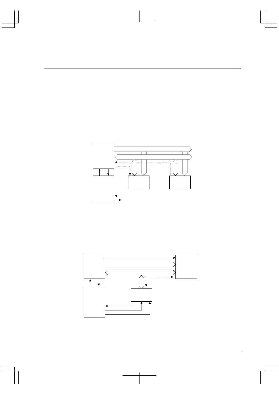
Dual-address transfer
In this method, a source address and a destination address for DMA transfer can be specified and a DMA
transfer is performed in two phases. The first phase reads data at the source address into the on-chip temporary
register. The second phase writes the temporary register data to the destination address.
Unlike IDMA (Intelligent DMA), which has transfer information in memory, this DMA method does not
support a DMA link function but allows high-speed data transfers because it is not necessary to read transfer
information from a memory.
Memory, I/O
Data bus
Address bus
BCU
Memory, I/O
Data transfer
(1)
(2)
Source
Destination
High-speed
DMA
DMA request
End of DMA
#DMAREQx
#DMAENDx
Figure 2.1 Dual-Address Transfer Method
Single-address transfer
In this method, data transfers that are normally accomplished by executing data read and write operations
back-to-back are executed on the external bus collectively at one time, thus further speeding up the transfer
operation. The #DMAACKx and #DMAENDx signals are used to control data transfer.
Unlike dual-address transfer, this method does not allow memory to memory data transfer but data transfers
can be performed in minimum cycles.
High-speed
DMA
External I/O
Data bus
Address bus
BCU
Memory
I/O
Bus control signals
DMA request
DMA reception
End of DMA
#RD/#WR
#DMAREQx
#DMAACKx
#DMAENDx
Data transfer
Note:
Single-address mode
does not allow data transfer
between memory devices.
Figure 2.2 Single-Address Transfet Method
Note: Channels 0 to 3 are configured in the same way and have the same functionality. Signal and control
bit names are assigned channel numbers 0 to 3 to distinguish them from other channels. In this
manual, however, channel numbers 0 to 3 are designated with an "x" except where they must be
distinguished, as the explanation is the same for all channels.