I/o ports (p ports), Structure of i/o port, I/o port pins – Epson S1C33210 User Manual
Page 366
III PERIPHERAL BLOCK: INPUT/OUTPUT PORTS
B-III-9-4
EPSON
S1C33210 FUNCTION PART
I/O Ports (P Ports)
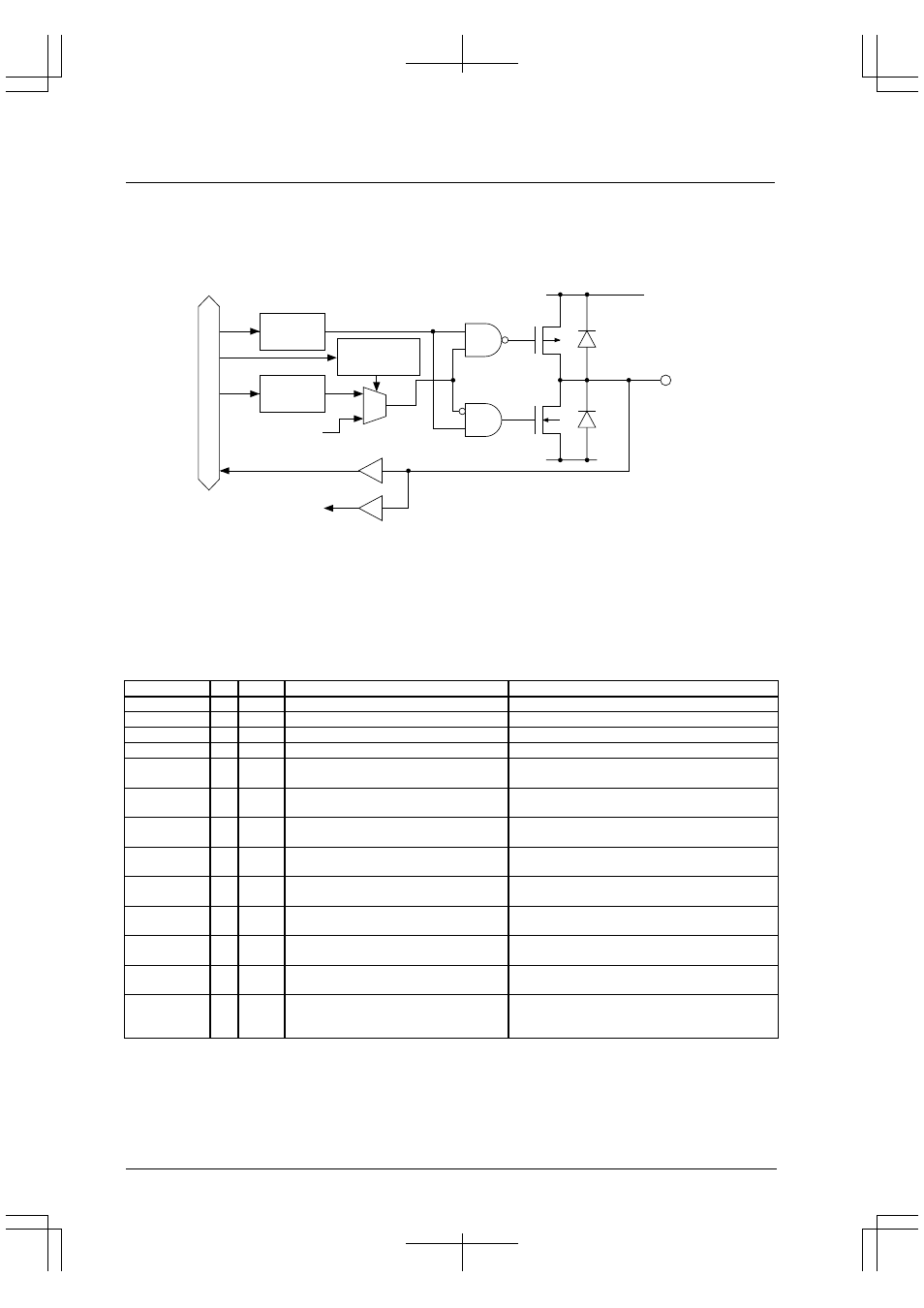
Structure of I/O Port
The Peripheral Block contains 29 bits of I/O ports (P00 to P05, P10 to P16, P20 to P27, P30 to P35) that can be
directed for input or output through the use of a program.
Figure 9.2 shows the structure of a typical I/O port.
V
DDE
V
SS
Internal data bus
Pxx
Data
register
Peripheral circuit
input
Peripheral circuit
output
I/O control
register
Function
select register
Figure 9.2 Structure of I/O Port
I/O Port Pins
The I/O ports concurrently serve as the input/output pins for peripheral circuits, as shown in Table 9.3. Whether they
are used as I/O ports or for peripheral circuits can be set bit-for-bit using a function select register. All pins not used
for peripheral circuits can be used as general-purpose I/O ports.
Table 9.3 I/O Pins
Pin name
I/O
Pull-up
Function
Function select bit
P00/SIN0
I/O
–
I/O port / Serial IF Ch.0 data input
CFP00(D0)/P0 function select register(0x402D0)
P01/SOUT0
I/O
–
I/O port / Serial IF Ch.0 data output
CFP01(D1)/P0 function select register(0x402D0)
P02/#SCLK0
I/O
–
I/O port / Serial IF Ch.0 clock input/output
CFP02(D2)/P0 function select register(0x402D0)
P03/#SRDY0
I/O
–
I/O port / Serial IF Ch.0 ready input/output
CFP03(D3)/P0 function select register(0x402D0)
P04/SIN1
I/O
–
I/O port / Serial IF Ch.1 data input
CFP04(D4)/P0 function select register(0x402D0)
CFEX4(D4)/Port function extension register(0x402DF)
P05/SOUT1
I/O
–
I/O port / Serial IF Ch.1 data output
CFP05(D5)/P0 function select register(0x402D0)
CFEX5(D5)/Port function extension register(0x402DF)
P10/EXCL0/
T8UF0/DST0
∗
I/O
–
I/O port / 16-bit timer 0 event counter input (I) /
8-bit timer 0 output (O) / DST0 output (Ex)
CFP10(D0)/P1 function select register(0x402D4)
CFEX1(D1)/Port function extension register(0x402DF)
P11/EXCL1/
T8UF1/DST1
∗
I/O
–
I/O port / 16-bit timer 1 event counter input (I) /
8-bit timer 1 output (O) / DST1 output (Ex)
CFP11(D1)/P1 function select register(0x402D4)
CFEX1(D1)/Port function extension register(0x402DF)
P12/EXCL2/
T8UF2/DST2
∗
I/O
–
I/O port / 16-bit timer 2 event counter input (I) /
8-bit timer 2 output (O) / DST2 output (Ex)
CFP12(D2)/P1 function select register(0x402D4)
CFEX0(D0)/Port function extension register(0x402DF)
P13/EXCL3/
T8UF3/DPCO
∗
I/O
–
I/O port / 16-bit timer 3 event counter input (I) /
8-bit timer 3 output (O) / DPCO output (Ex)
CFP13(D3)/P1 function select register(0x402D4)
CFEX1(D1)/Port function extension register(0x402DF)
P14/FOSC1/
DCLK
∗
I/O
–
I/O port / Low-speed (OSC1) clock output /
DCLK output (Ex)
CFP14(D4)/P1 function select register(0x402D4)
CFEX0(D0)/Port function extension register(0x402DF)
P15/EXCL4/
#DMAEND0
I/O
–
I/O port / 16-bit timer 4 event counter input (I) /
#DMAEND0 output (O)
CFP15(D5)/P1 function select register(0x402D4)
P16/EXCL5/
#DMAEND1/
SOUT3
I/O
–
I/O port / 16-bit timer 5 event counter input (I) /
#DMAEND1 output (O) / Serial IF Ch.3 data
output
CFP16(D6)/P1 function select register(0x402D4)
(I): Input mode, (O): Output mode, (Ex): Extended function
∗
: A 3-V system I/O voltage can only be used for the P10–P14 pins.