I/o memory of bcu – Epson S1C33210 User Manual
Page 185

II CORE BLOCK: BCU (Bus Control Unit)
S1C33210 FUNCTION PART
EPSON
B-II-4-33
I/O Memory of BCU
Table 4.21 shows the control bits of the BCU. These I/O memories are mapped into the area (0x48000 and following
addresses) used for the internal 16-bit peripheral circuits. However, these I/O memories can be accessed in bytes or
words, as well as in half-words.
For the control bits of the external system interface pins assigned to the I/O ports, and for details on how to control
the 8-bit programmable timer 0 in order to generate a DRAM refresh cycle, refer to each corresponding section in
this manual.
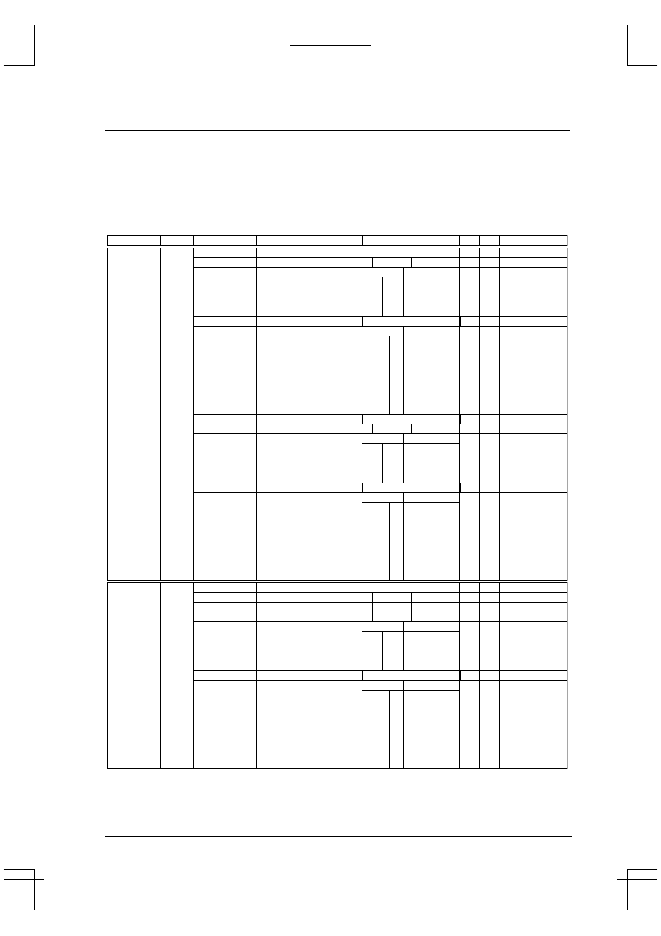
Table 4.21 Control Bits of External System Interface
Name
Address
Register name
Bit
Function
Setting
Init.
R/W
Remarks
–
–
A18SZ
A18DF1
A18DF0
–
A18WT2
A18WT1
A18WT0
–
A16SZ
A16DF1
A16DF0
–
A16WT2
A16WT1
A16WT0
DF
DE
DD
DC
DB
DA
D9
D8
D7
D6
D5
D4
D3
D2
D1
D0
reserved
Areas 18–17 device size selection
Areas 18–17
output disable delay time
reserved
Areas 18–17 wait control
reserved
Areas 16–15 device size selection
Areas 16–15
output disable delay time
reserved
Areas 16–15 wait control
–
–
–
1 8 bits
0 16 bits
1 8 bits
0 16 bits
–
0
1
1
–
1
1
1
–
0
1
1
–
1
1
1
–
R/W
R/W
–
R/W
–
R/W
R/W
–
R/W
0 when being read.
0 when being read.
0 when being read.
0 when being read.
0048120
(HW)
Areas 18–15
set-up register
1
1
0
0
1
0
1
0
A18DF[1:0] Number of cycles
3.5
2.5
1.5
0.5
1
1
0
0
1
0
1
0
A16DF[1:0] Number of cycles
3.5
2.5
1.5
0.5
1
1
1
1
0
0
0
0
1
1
0
0
1
1
0
0
1
0
1
0
1
0
1
0
A18WT[2:0]
Wait cycles
7
6
5
4
3
2
1
0
1
1
1
1
0
0
0
0
1
1
0
0
1
1
0
0
1
0
1
0
1
0
1
0
A16WT[2:0]
Wait cycles
7
6
5
4
3
2
1
0
–
A14DRA
A13DRA
A14SZ
A14DF1
A14DF0
–
A14WT2
A14WT1
A14WT0
DF–9
D8
D7
D6
D5
D4
D3
D2
D1
D0
reserved
Area 14 DRAM selection
Area 13 DRAM selection
Areas 14–13 device size selection
Areas 14–13
output disable delay time
reserved
Areas 14–13 wait control
–
–
1 Used
0 Not used
1 Used
0 Not used
1 8 bits
0 16 bits
–
0
0
0
1
1
–
1
1
1
–
R/W
R/W
R/W
R/W
–
R/W
0 when being read.
0 when being read.
0048122
(HW)
1
1
0
0
1
0
1
0
A14DF[1:0] Number of cycles
3.5
2.5
1.5
0.5
1
1
1
1
0
0
0
0
1
1
0
0
1
1
0
0
1
0
1
0
1
0
1
0
A14WT[2:0]
Wait cycles
7
6
5
4
3
2
1
0
Areas 14–13
set-up register
