Epson S1C33210 User Manual
Page 136
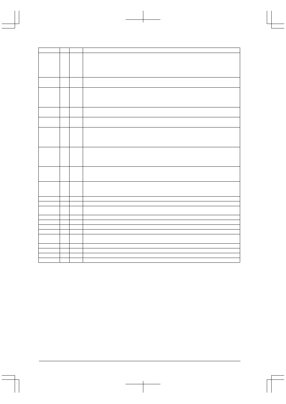
I OUTLINE: LIST OF PINS
B-I-3-4
EPSON
S1C33210 FUNCTION PART
Pin name
I/O
Pull-up
Function
P16
EXCL5
#DMAEND1
I/O
–
P16:
I/O port when CFP16(D6/0x402D4) = "0" (default)
EXCL5:
16-bit timer 5 event counter input when CFP16(D6/0x402D4) = "1" and IOC16(D6/0x402D6)
= "0"
#DMAEND1: HSDMA Ch. 1 end-of-transfer signal output when CFP16(D6/0x402D4) = "1" and
IOC16(D6/0x402D6) = "1"
P20
#DRD
I/O
–
P20:
I/O port when CFP20(D0/0x402D8) = "0" (default)
#DRD:
DRAM read signal output for successive RAS mode when CFP20(D0/0x402D8) = "1"
P21
#DWE
#GAAS
I/O
–
P21:
I/O port when CFP21(D1/0x402D8) = "0" and CFEX2(D2/0x402DF) = "0" (default)
#DWE: DRAM
read
signal
output
for
successive
RAS
mode
when
CFP21(D1/0x402D8)
=
"1"
and
CFEX2(D2/0x402DF) = "0"
#GAAS: Area
address
strobe
for
GA
when
CFEX2(D2/0x402DF)
=
"1"
P22
TM0
I/O
–
P22:
I/O port when CFP22(D2/0x402D8) = "0" (default)
TM0:
16-bit timer 0 output when CFP22(D2/0x402D8) = "1"
P23
TM1
I/O
–
P23:
I/O port when CFP23(D3/0x402D8) = "0" (default)
TM1:
16-bit timer 1 output when CFP23(D3/0x402D8) = "1"
P24
TM2
#SRDY2
I/O
–
P24:
I/O port when CFP24(D4/0x402D8) = "0" (default)
TM2:
16-bit timer 2 output when CFP24(D4/0x402D8) = "1"
#SRDY2:
Serial I/F Ch.2 ready signal input/output when SSRDY2(D3/0x402DB) = "1" and CFP24
(D4/0x402D8) = "0"
P25
TM3
#SCLK2
I/O
–
P25:
I/O port when CFP25(D5/0x402D8) = "0" (default)
TM3:
16-bit timer 3 output when CFP25(D5/0x402D8) = "1"
#SCLK2:
Serial I/F Ch.2 clock input/output when SSCLK2(D2/0x402DB) = "1" and
CFP25(D5/0x402D8) = "0"
P26
TM4
SOUT2
I/O
–
P26:
I/O port when CFP26(D6/0x402D8) = "0" (default)
TM4:
16-bit timer 4 output when CFP26(D6/0x402D8) = "1"
SOUT2:
Serial I/F Ch.2 data output when SSOUT2(D1/0x402DB) = "1" and CFP26(D6/0x402D8) = "0"
P27
TM5
SIN2
I/O
–
P27:
I/O port when CFP27(D7/0x402D8) = "0" (default)
TM5:
16-bit timer 5 output when CFP27(D7/0x402D8) = "1"
SIN2:
Serial I/F Ch.2 data input when SSIN2(D0/0x402DB) = "1" and CFP27(D7/0x402D8) = "0"
DTR
O
–
DTR output
*
1
RTS
O
–
RTS output
*
1
TXD
SOUT3
O
–
TXD:
TXD output
*
1 when MSEL pin input is at High level
SOUT3:
SOUT3 output when MSEL pin input is at Low level
RI
I
–
RI input
*
1
CTS
I
–
CTS input
*
1
DCD
I
–
DCD input
*
1
DSR
I
–
DSR input
*
1
RXD
SIN3
I
–
RXD:
RXD input when MSEL pin input is at High level
SIN3:
SIN3 input when MSEL pin input is at Low level
CNT1
O
–
Mobile access control output #1
CNT2
O
–
Mobile access control output #2
MSEL
I
Pull-up Serial I/O interface Ch. 3 configuration input. Normally drive this at High level.
GOUT
O
–
NMI interrupt request output
Note:
*
1 The communications macro select (MCRS) register (D[1:0]/0x200000) configures the I/O
signals to match the target mobile device.