External memory map and chip enable – Epson S1C33210 User Manual
Page 157
II CORE BLOCK: BCU (Bus Control Unit)
S1C33210 FUNCTION PART
EPSON
B-II-4-5
External Memory Map and Chip Enable
The BCU has a 24-bit external address bus (A[23:0]) and a 16-bit external data bus (D[15:0]), allowing an address
space of up to 16 MB to be accessed with one chip enable signal. By default, the address space is divided into 11
areas (areas 0 to 10) for management purposes. Of these, areas 4 to 10 are open to an external system, each provided
with an independent chip-enable pin (#CE[10:4]).
The C33 Core Block is limited to 24 available pins for the address bus and 7 pins for the #CE output due to its
package structure. However, the #CE[4:10] output pins can be switched to the high-order area chip enable output
pins as shown in Table 4.5 using software. CEFUNC[1:0] (D[A:9]) / DRAM timing set-up register (0x48130) is used
for this switching.
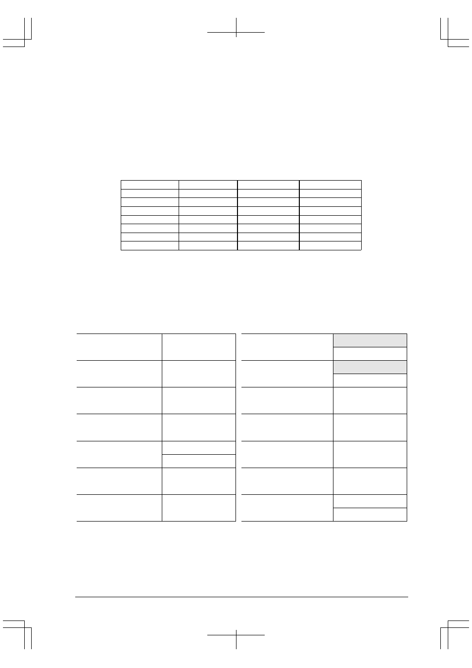
Table 4.5 Switching of #CE Output
Pin
CEFUNC = "00"
CEFUNC = "01"
CEFUNC = "1x"
#CE4
#CE4
#CE11
#CE11+#CE12
#CE5
#CE5
#CE15
#CE15+#CE16
#CE6
#CE6
#CE6
#CE7+#CE8
#CE7/#RAS0
#CE7/#RAS0
#CE13/#RAS2
#CE13/#RAS2
#CE8/#RAS1
#CE8/#RAS1
#CE14/#RAS3
#CE14/#RAS3
#CE9
#CE9
#CE17
#CE17+#CE18
#CE10EX
#CE10EX
#CE10EX
#CE9+#CE10EX
(Default: CEFUNC = "00")
The high-order areas that are made available for use by writing "01" to CEFUNC can be larger in size than the default
low-order areas. For example, when using DRAM in default settings, the available space is 4 MB in areas 7 and 8.
However, if areas 13 and 14 are used, up to 32 MB of DRAM can be used. The same applies to the other areas.
Furthermore, when CEFUNC is set to "10" or "11", five chip enable signals are expanded into two area size.
Although the C33 Core Block has only 24 address output pins, it features 28-bit internal address processing.
Figure 4.2 shows a memory map for an external system.
0x0FFFFFF
0x0C00000
0x0BFFFFF
0x0800000
0x07FFFFF
0x0600000
0x05FFFFF
0x0400000
0x03FFFFF
0x0380000
0x037FFFF
0x0300000
0x02FFFFF
0x0200000
0x01FFFFF
0x0100000
Area
Area 10
(#CE10)
SRAM type
Burst ROM type
8 or 16 bits
Area 9
(#CE9)
SRAM type
Burst ROM type
8 or 16 bits
Area 8
(#CE8/#RAS1)
SRAM type
DRAM type
8 or 16 bits
Area 7
(#CE7/#RAS0)
SRAM type
DRAM type
8 or 16 bits
Area 6
(#CE6)
SRAM type
Area 5
(#CE5)
SRAM type
Area 4
(#CE4)
SRAM type
8 or 16 bits
Area
Area 17
(#CE17)
SRAM type
8 or 16 bits
Area 15
(#CE15)
SRAM type
8 or 16 bits
Area 14
(#CE14/#RAS3)
SRAM type
DRAM type
8 or 16 bits
Area 13
(#CE13/#RAS2)
SRAM type
DRAM type
8 or 16 bits
Area 11
(#CE11)
SRAM type
8 or 16 bits
Area 10
(#CE10)
SRAM type
Burst ROM type
8 or 16 bits
Area 6
(#CE6)
SRAM type
Address
External memory 1 (1MB)
Internal I/O memory
External memory 3 (2MB)
External memory 4 (2MB)
External memory 5 (4MB)
External memory 6 (4MB)
External I/O (8-bit device)
External I/O (16-bit device)
0xBFFFFFF
0x9000000
0x8FFFFFF
0x8000000
0x5FFFFFF
0x5000000
0x4FFFFFF
0x4000000
0x3FFFFFF
0x3000000
0x2FFFFFF
0x2000000
0x17FFFFF
0x1000000
0x0FFFFFF
0x0C00000
0x03FFFFF
0x0380000
0x037FFFF
0x0300000
Address
External memory 3 (16MB)
External memory 4 (16MB)
External memory 5 (16MB)
External memory 6 (16MB)
(Mirror of External memory 6)
(Mirror of External memory 5)
External I/O (8-bit device)
External I/O (16-bit device)
External memory 1 (4MB)
External memory 2 (8MB)
CEFUNC = "00"
CEFUNC = "01"