Epson S1C33210 User Manual
Page 348
III PERIPHERAL BLOCK: SERIAL INTERFACE
B-III-8-32
EPSON
S1C33210 FUNCTION PART
Name
Address
Register name
Bit
Function
Setting
Init.
R/W
Remarks
–
CFP05
CFP04
CFP03
CFP02
CFP01
CFP00
D7-6
D5
D4
D3
D2
D1
D0
Reserved
P05 function selection
P04 function selection
P03 function selection
P02 function selection
P01 function selection
P00 function selection
–
0
0
0
0
0
0
–
R/W
R/W
R/W
R/W
R/W
R/W
0 when being read.
Extended functions
(0x402DF)
00402D0
(B)
–
1 SOUT1
0 P05
1 SIN1
0 P04
1 #SRDY0
0 P03
1 #SCLK0
0 P02
1 SOUT0
0 P01
1 SIN0
0 P00
P0 function
select register
–
CFP322
CFP152
CFP162
CFP332
D7–4
D3
D2
D1
D0
reserved
P32 function selection 2
P15 function selection 2
P16 function selection 2
P33 function selection 2
–
–
0
0
0
0
–
R/W
R/W
R/W
R/W
00402D7
Port SIO
function
extension
register
1
–
0 P32/
#DMAACK0
1
–
0 P15/EXCL4/
#DMAEND0
1
–
0 P16/EXCL5/
#DMAEND1
1
–
0 P33/
#DMAACK1
Always set to 0.
Always set to 0.
Always set to 0.
Always set to 0.
–
SSRDY2
SSCLK2
SSOUT2
SSIN2
D7–4
D3
D2
D1
D0
reserved
Serial I/F Ch.2 SRDY selection
Serial I/F Ch.2 SCLK selection
Serial I/F Ch.2 SOUT selection
Serial I/F Ch.2 SIN selection
–
0
0
0
0
–
R/W
R/W
R/W
R/W
00402DB
1 #SRDY2
0 P24/TM2
1 #SCLK2
0 P25/TM3
1 SOUT2
0 P26/TM4
1 SIN2
0 P27/TM5
Port SIO
function
extension
register
–
–
CFEX5
CFEX4
CFEX3
CFEX2
CFEX1
CFEX0
D7-6
D5
D4
D3
D2
D1
D0
reserved
P05 port extended function
P04 port extended function
P31 port extended function
P21 port extended function
P10, P11, P13 port extended
function
P12, P14 port extended function
0
0
0
0
0
1
1
R/W
R/W
R/W
R/W
R/W
R/W
R/W
Undefined when read.
Always set to 0.
Always set to 0.
00402DF
(B)
Port function
extension
register
1
1
–
0 P05, etc.
1
–
0 P04, etc.
1 #GARD
0 P31, etc.
1 #GAAS
0 P21, etc.
1 DST0
DST1
DPC0
0 P10, etc.
P11, etc.
P13, etc.
1 DST2
DCLK
0 P12, etc.
P14, etc.
–
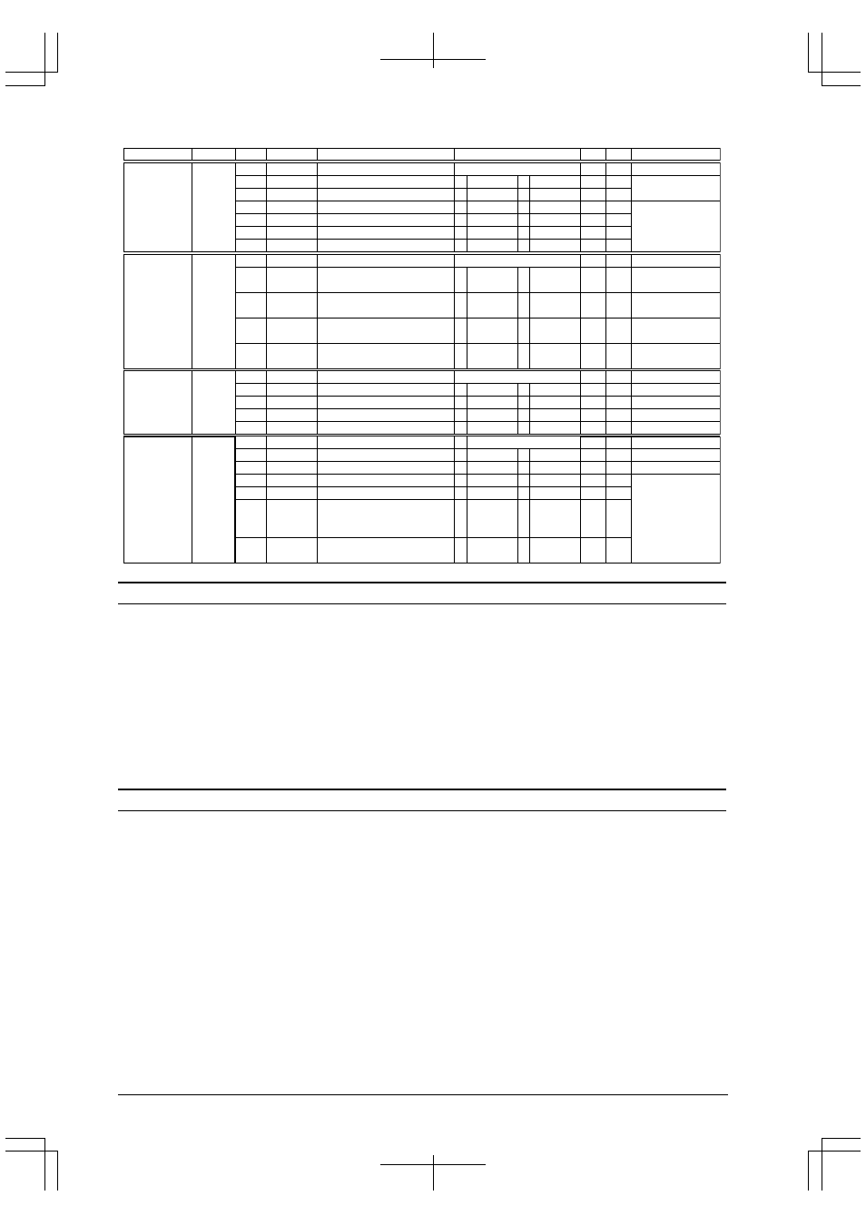
CFP05–CFP00: P0[5:0] pin function selection (D[5:0]) / P0 function select register (0x402D0)
Selects the pins used for the serial interface.
Write "1": Serial-interface input/output pin
Write "0": I/O port pin
Read: Valid
Select the pins used for the serial interface from among P00 through P05 by writing "1" to CFP00 through CFP07.
P00–P03 (SIN0, SOUT0, #SCLK0, #SRDY0) are used for channel 0; P04–P05 (SIN1, SOUT1) are used for channel
1. If the bit for a pin is set to "0", the pin functions as an I/O port.
The necessary input/output pins differ depending on the transfer mode set (see Table 8.3).
At cold start, CFP is set to "0" (I/O port). At hot start, CFP retains its state from prior to the initial reset.
CFP332: P33 function selection 2 (D0) / Port SIO function extension register (0x402D7)
Specifies the function of pin P33/#DMAACK1. Always set to "0."
Write "0": P33/#DMAACK1
Read: Valid
To use the pin as P33 or #DMAACK1, set this bit to "0".
At power-on, this bit is set to "0".