Iii-3 8-bit programmable timers, Configuration of 8-bit programmable timer, Output pins of 8-bit programmable timers – Epson S1C33210 User Manual
Page 249
III PERIPHERAL BLOCK: 8-BIT PROGRAMMABLE TIMERS
S1C33210 FUNCTION PART
EPSON
B-III-3-1
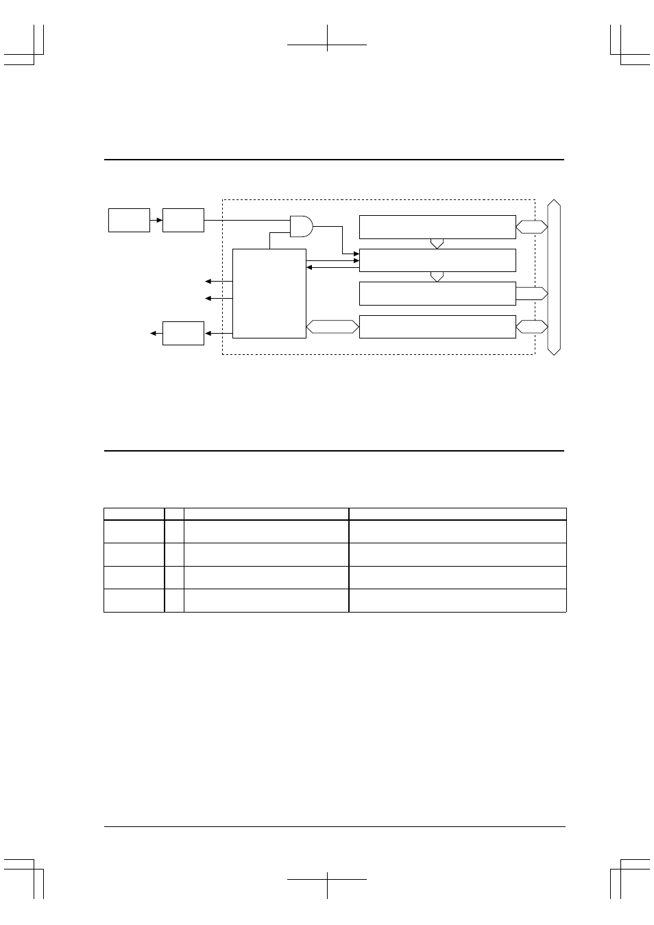
III-3 8-BIT PROGRAMMABLE TIMERS
Configuration of 8-Bit Programmable Timer
The Peripheral Block contains six channels of 8-bit programmable timers (timers 0 to 5).
Figure 3.1 shows the structure of the 8-bit programmable timer.
Data bus
8-bit reload data register (RLDx)
8-bit down counter
Control registers
Control circuit
Data buffer (PTDx)
Underflow
Reload
Clock output
Underflow signal output
Underflow
interrupt
Interrupt
controller
Prescaler
Clock
generator
Figure 3.1 Structure of 8-Bit Programmable Timer
Each timer consists of an 8-bit presentable counter and can output a clock generated by the counter's underflow
signal to the internal peripheral circuits or external devices. The output clock cycle can be selected from a wide range
of cycles by setting the preset data that can be set in the software and the input clock in the prescaler.
Output Pins of 8-Bit Programmable Timers
The underflow signals of 8-bit programmable timers 0 to 3 can be output to external devices.
Table 3.1 shows the pins that are used to output the underflow signals of the 8-bit programmable timers to external
devices.
Table 3.1 Output Pins of 8-Bit Programmable Timers
Pin name
I/O
Function
Function select bit
P10/EXCL0/
T8UF0
I/O I/O port / 16-bit timer 0 event counter
input / 8-bit timer 0 output / DST0 output
CFP10(D0)/P1 function select register (0x402D4)
CFEX1(D1)/Port function extension register (0x402DF)
P11/EXCL1/
T8UF1
I/O I/O port / 16-bit timer 1 event counter
input / 8-bit timer 1 output / DST1 output
CFP11(D1/P1 function select register (0x402D4)
CFEX1(D1)/Port function extension register (0x402DF)
P12/EXCL2/
T8UF2
I/O I/O port / 16-bit timer 2 event counter
input / 8-bit timer 2 output / DST2 output
CFP12(D2/P1 function select register (0x402D4)
CFEX0(D0)/Port function extension register (0x402DF)
P13/EXCL3/
T8UF3
I/O I/O port / 16-bit timer 3 event counter
input / 8-bit timer 3 output / DPCO output
CFP13(D3/P1 function select register (0x402D4)
CFEX1(D1)/Port function extension register (0x402DF)
T8UFx (output pin of the 8-bit programmable timer)
This pin outputs a clock divided in each 8-bit programmable timer. The pulse width is equal to that of input
clock of the 8-bit programmable timer (prescaler output). Therefore, the pulse width varies according to the
prescaler setting.
How to set the output pins of the 8-bit programmable timer
All pins used by the 8-bit programmable timers are shared with I/O ports, event counter inputs of the 16-bit
programmable timers and debug signal outputs. At cold start, all these pins are set for the debug signal outputs
(function select bit CFP1[3:0] = "0", port extended function bit CFEX[1:0] = "1"). When using the clock output
function of the 8-bit programmable timer, write "0" to the port extended function bit CFEXx and write "1" to
the function select bit CFP1x for the corresponding pin.
Then, after setting the above, write "1" to the I/O port's I/O control bit IOC1x (D[3:0]) / P1 I/O control register
(0x402D6) to set to output mode. In input mode, the pin functions as the 16-bit programmable timer's event
counter input and cannot be used to output a clock of the 8-bit programmable timer. At cold start, the register is
set to input mode. At hot start, the register retains its status from prior to the reset.