Epson S1C33210 User Manual
Page 413
III PERIPHERAL BLOCK: MONITORED MOBILE ACCESS INTERFACES
S1C33210 FUNCTION PART
EPSON
B-III-10-27
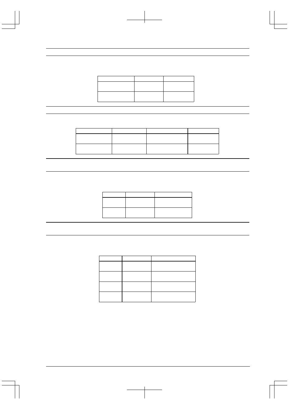
CNT2, CNT1: Output port data (D[1:0]) /Communications block output port data register (0x020000A)
Regardless of the communications macro select (MCRS) register (D[1:0]/0x200000) setting–that is, in all modes–
these bits drive the CNT2 and CNT1 output pins using negative logic. (See Table.)
Table 10.16 Communications Block Outputs CNT2 and CNT1
Output port data
Output pins
Output level
CNT2 = 1
CNT2 = 0
CNT2
Low
High
CNT1 = 1
CNT1 = 0
CNT1
Low
High
GOUTE: GOUT output enable (D7) / Communications block input port data register (0x020000C)
Setting this bit to "1" connects the RI input to the GOUT output pin.
Table 10.17 Communications Block Output GOUT
GOUTE setting
RI input level
GOUT output level
Notes
GOUTE = 1
High
Low
High
Low
Pass through
output
GOUTE = 0
High
Low
High
High
Output disabled
MIPORT1, MIPORT0: Input port data (D[1:0]) / Communications block input port data register
(0x020000C)
Regardless of the communications macro select (MCRS) register (D[1:0]/0x200000) setting–that is, in all modes–
these bits track the input levels for the corresponding pins.
Table 10.18 Communications Block Inputs DSR and RI
Input pin
Input Level
Register Data
DSR
High
Low
MIPORT1 = 1
MIPORT1 = 0
RI
High
Low
MIPORT0 = 1
MIPORT0 = 0
RI, CTS, DCD, DSR: Modem status (D[11:8]) / Communications block modem status register
(0x020002A)
Regardless of the communications macro select (MCRS) register (D[1:0]/0x200000) setting–that is, in all modes–
these bits track the input levels for the corresponding pins using negative logic. Writes to these bits are ignored.
Table 10.19 Communications Block Modem Status
Input pin
Input Level
Register Data
RI
High
Low
RI = 0
RI = 1
CTS
High
Low
CTS = 0
CTS = 1
DCD
High
Low
DCD = 0
DCD = 1
DSR High
Low
DSR = 0
DSR = 1