Epson S1C33210 User Manual
Page 105
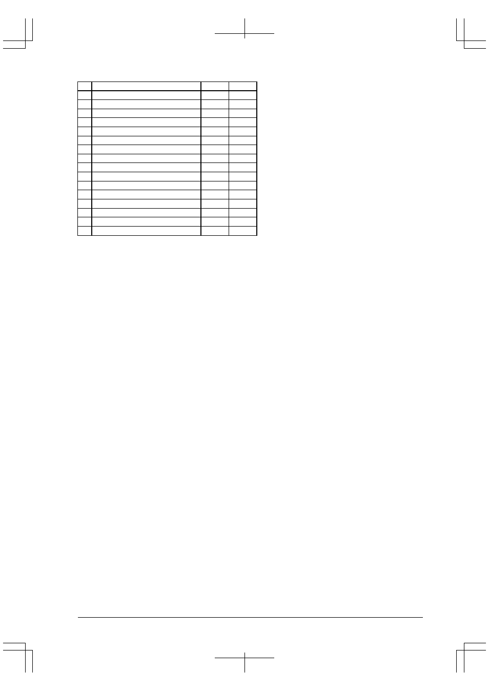
10 PAD LAYOUT
S1C33210 PRODUCT PART
EPSON
A-91
No.
Pad name
X
Y
201 N.C.
-2.834
-0.966
202 P23/TM1
-2.834
-1.05
203 N.C.
-2.834
-1.134
204 DSIO
-2.834
-1.218
205 N.C.
-2.834
-1.302
206 P10/EXCL0/T8UF0/DST0
-2.834
-1.386
207 P11/EXCL1/T8UF1/DST1
-2.834
-1.47
208 N.C.
-2.834
-1.554
209 P12/EXCL2/T8UF2/DST2
-2.834
-1.638
210 P13/EXCL3/T8UF3/DPC0
-2.834
-1.722
211 P14/FOSC1/DCLK
-2.834
-1.806
212 P24/TM2/#SRDY2
-2.834
-1.89
213 N.C.
-2.834
-1.974
214 P25/TM3/#SCLK2
-2.834
-2.058
215 N.C.
-2.834
2.154
216 N.C.
-2.834
-2.154
Note: The S1C33210 is constructed with 0.35
µ
m process technology. Since the pad pitch is to small, it is
impossible to use all pads when mounting the chip (die form) on the board. When mounting the
chip use the pads other than "N.C." and "N.C. (xxxx)". The pads which is indicated with "N.C.
(xxxx)" in the table is available in the QFP15-128pin package.