Epson S1C33210 User Manual
Page 137
I OUTLINE: LIST OF PINS
S1C33210 FUNCTION PART
EPSON
B-I-3-5
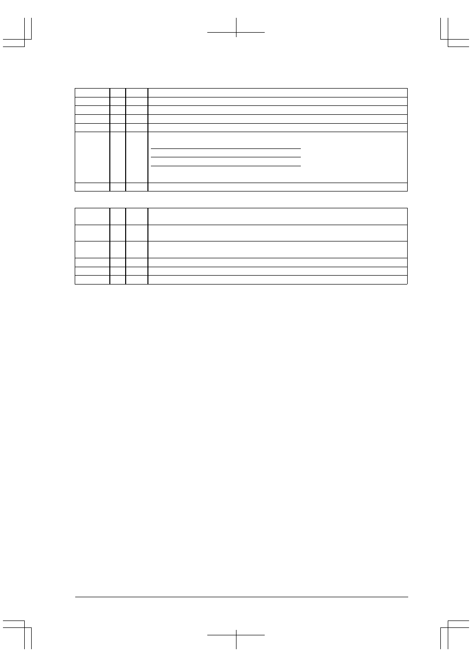
Table 3.4 List of Pins for Clock Generator
Pin name
I/O
Pull-up
Function
OSC1
I
–
Low-speed (OSC1) oscillation input (32 kHz crystal oscillator or external clock input)
OSC2
O
–
Low-speed (OSC1) oscillation output
OSC3
I
–
High-speed (OSC3) oscillation input (crystal/ceramic oscillator or external clock input)
OSC4
O
–
High-speed (OSC3) oscillation output
PLLS[1:0]
I
–
PLL set-up pins
PLLS1
PLLS0
fin (f
OSC3
)
fout (f
PSCIN
)
1
1
10–25MHz
20–50MHz
0
1
10–12.5MHz
40–50MHz
0
0
PLL is not used
L
PLLC
–
–
Capasitor connecting pin for PLL
Table 3.5 List of Other Pins
Pin name
I/O
Pull-up
Function
/down
TST
I
Pull-
down
Test mode input pin
This pin is used for testing this chip. For further details, refer to the S1C33 ASIC Design Guide.
DSIO
I/O
Pull-up Serial I/O pin for debugging
This pin is used to communicate with the debugging tool S5U1C33000H.
#X2SPD
I
–
Clock doubling mode set-up pin1: CPU clock = bus clock
×
1, 0: CPU clock = bus clock
×
2
#NMI
I
Pull-up NMI request input pin
#RESET
I
Pull-up Initial reset input pin
Note: "#" in the pin names indicates that the signal is low active.