Epson S1C33210 User Manual
Page 331
III PERIPHERAL BLOCK: SERIAL INTERFACE
S1C33210 FUNCTION PART
EPSON
B-III-8-15
• Sampling clock
In the asynchronous mode, TCLK (the clock output by the 8-bit programmable timer or input from the #SCLKx
pin for Ch. 0 and Ch. 2) is internally divided in the serial interface, in order to create a sampling clock.
A 1/16 division ratio is selected by writing "0" to DIVMDx , and a 1/8 ratio is selected by writing "1".
Ch.0 clock division ratio selection: DIVMD0 (D4) / Serial I/F Ch.0 IrDA register (0x401E4)
Ch.1 clock division ratio selection: DIVMD1 (D4) / Serial I/F Ch.1 IrDA register (0x401E9)
Ch.2 clock division ratio selection: DIVMD2 (D4) / Serial I/F Ch.2 IrDA register (0x401F4)
Ch.3 clock division ratio selection: DIVMD3 (D4) / Serial I/F Ch.3 IrDA register (0x401F9)
Note: The DIVMDx bit becomes indeterminate at initial reset, so be sure to reset it in the software.
Settings of this bit are valid only in the asynchronous mode (and when using the IrDA interface).
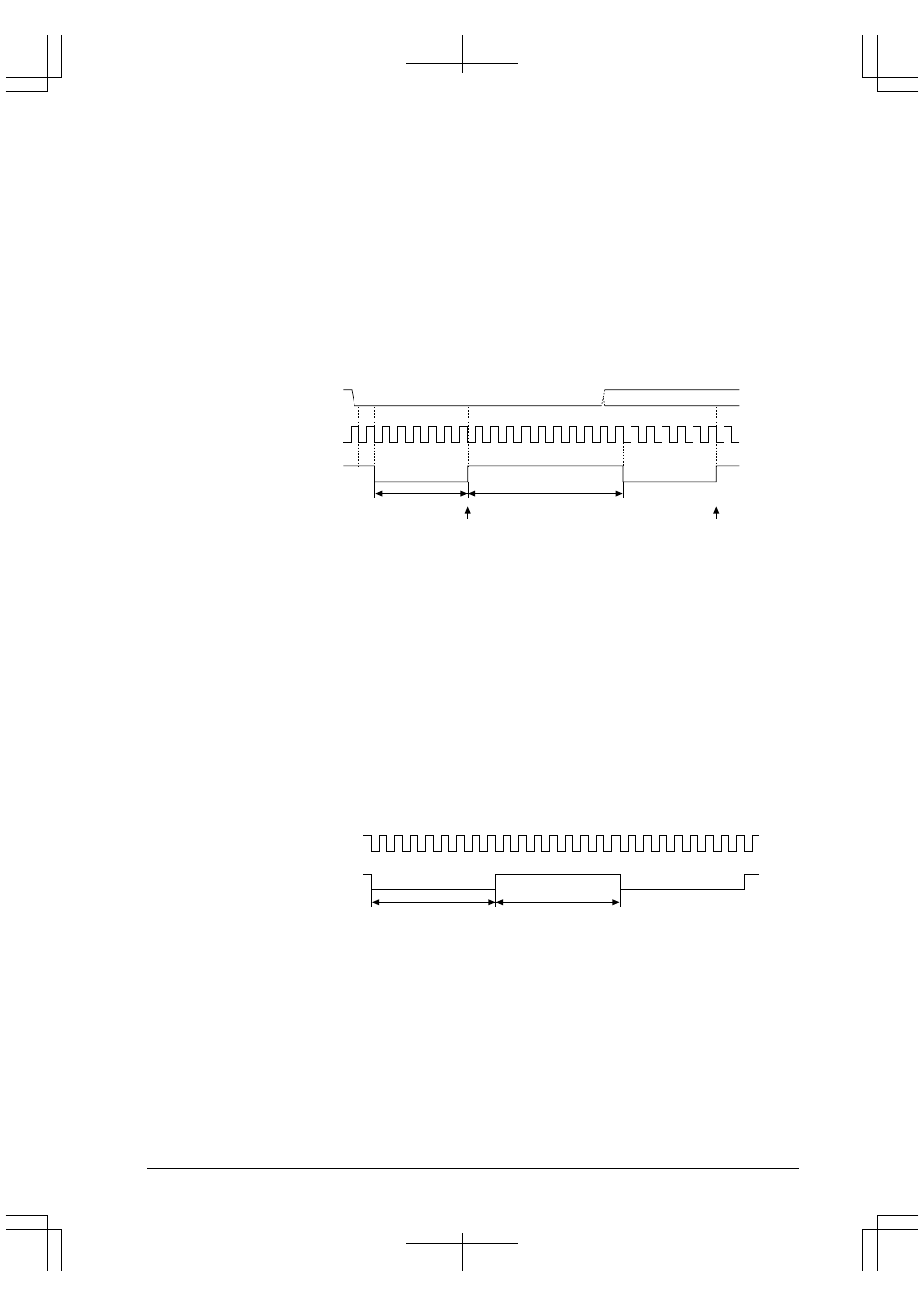
For receiving
SINx
TCLK
Sampling clock for receiving
Sampling of start bit
Start bit
D0
1
2
6
×
TCLK
10
×
TCLK
1
2
8
8
16
Sampling of D0 bit
Figure 8.10 Sampling Clock for Asynchronous Receive Operation (when 1/16 division is selected)
As shown in Figure 8.10, the sampling clock is created by dividing TCLK by 16 (or 8). Its duty ratio (low: high
ratio) is 6:10 (or 2:6 when divided by 8), and not 50%. Since the receive data is sampled in the middle point of
each bit, the sampling clock recognizes the start bit first, and then changes the level from high to low at the
second falling edge of TCLK. And at the 8th (4th for 1/8) falling edge of TCLK, it changes the level from low
to high. This change in levels is repeated for the following bits of data:
Each bit of data is sampled at each rising edge of this sampling clock. When the stop bit is sampled, the
sampling clock is fixed at high level until the next start bit is sampled.
If the SINx pin is returned to high level at the second falling edge of TCLK when it recognize the start bit, the
data is assumed to be noise, and generation of the sampling clock is stopped.
If the SINx pin is not on a low level when the start bit is sampled at the 8th (4th for 1/8) clock, such as when the
baud rate is not matched between the transmit and receive units, the serial interface stops sampling the
following data and returns to a start-bit detection mode. In this case, no error is generated.
For transmitting
TCLK
Sampling clock for transmitting
1
2 3
16
. . .
8
×
TCLK
8
×
TCLK
Figure 8.11 Sampling Clock for Asynchronous Transmit Operation (when 1/16 division is selected)
When transmitting data, a sampling clock of a 50% duty cycle is generated from TCLK by dividing it by 16 (or
8), and each bit of data is output synchronously with this clock.