Epson S1C33210 User Manual
Page 312
III PERIPHERAL BLOCK: CLOCK TIMER
B-III-7-8
EPSON
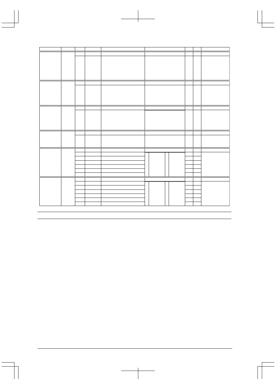
S1C33210 FUNCTION PART
Name
Address
Register name
Bit
Function
Setting
Init.
R/W
Remarks
0 to 59 minutes
(Note) Can be set within 0–63.
–
TCCH5
TCCH4
TCCH3
TCCH2
TCCH1
TCCH0
D7–6
D5
D4
D3
D2
D1
D0
reserved
Clock timer minute comparison
data
TCCH5 = MSB
TCCH0 = LSB
–
X
X
X
X
X
X
–
R/W
0 when being read.
0040159
(B)
–
Clock timer
minute
comparison
register
0 to 23 hours
(Note) Can be set within 0–31.
–
TCCD4
TCCD3
TCCD2
TCCD1
TCCD0
D7–5
D4
D3
D2
D1
D0
reserved
Clock timer hour comparison data
TCCD4 = MSB
TCCD0 = LSB
–
X
X
X
X
X
–
R/W
0 when being read.
004015A
(B)
–
Clock timer
hour
comparison
register
0 to 31 days
–
TCCN4
TCCN3
TCCN2
TCCN1
TCCN0
D7–5
D4
D3
D2
D1
D0
reserved
Clock timer day comparison data
TCCN4 = MSB
TCCN0 = LSB
–
X
X
X
X
X
–
R/W
0 when being read.
Compared with
TCND[4:0].
004015B
(B)
–
Clock timer
day
comparison
register
–
0 to 7
–
PCTM2
PCTM1
PCTM0
D7–3
D2
D1
D0
reserved
Clock timer interrupt level
–
X
X
X
–
R/W
Writing 1 not allowed.
004026B
(B)
Clock timer
interrupt
priority register
–
EP7
EP6
EP5
EP4
ECTM
EADE
D7–6
D5
D4
D3
D2
D1
D0
reserved
Port input 7
Port input 6
Port input 5
Port input 4
Clock timer
A/D converter
–
–
0
0
0
0
0
0
–
R/W
R/W
R/W
R/W
R/W
R/W
0 when being read.
0040277
(B)
1 Enabled
0 Disabled
Port input 4–7,
clock timer,
A/D interrupt
enable register
–
FP7
FP6
FP5
FP4
FCTM
FADE
D7–6
D5
D4
D3
D2
D1
D0
reserved
Port input 7
Port input 6
Port input 5
Port input 4
Clock timer
A/D converter
–
–
X
X
X
X
X
X
–
R/W
R/W
R/W
R/W
R/W
R/W
0 when being read.
0040287
(B)
1 Factor is
generated
0 No factor is
generated
Port input 4–7,
clock timer, A/D
interrupt factor
flag register
TCRST: Clock timer reset (D1) / Clock timer Run/Stop register (0x40151)
Resets the clock timer.
Write "1": The clock timer is reset
Write "0": Invalid
Read: Always "0"
The clock timer is reset by writing "1" to TCRST when the timer is inactive. All timer counters are cleared to "0".
The clock timer cannot be reset when in the RUN state, nor can it be reset at the same time it is made to RUN
through the execution of one write to address 0x40151. (The clock timer is started, but not reset.) In this case, first
reset the clock timer and then use another instruction to RUN the clock timer. When the counters are cleared as the
clock timer is reset, an interrupt may be generated, depending on the register settings. Therefore, before resetting the
clock timer, first disable the clock timer interrupt, and after resetting the clock timer, reset the interrupt factor flag
and the interrupt factor and alarm factor generation flags.
Writing "0" to TCRST results in No Operation. Since this TCRST is a write-only bit, its value when read is always
"0".
The clock timer is not reset by an initial reset.