Clock-synchronized interface, Outline of clock-synchronized interface – Epson S1C33210 User Manual
Page 320

III PERIPHERAL BLOCK: SERIAL INTERFACE
B-III-8-4
EPSON
S1C33210 FUNCTION PART
Clock-Synchronized Interface
Outline of Clock-Synchronized Interface
In the clock-synchronized transfer mode, 8 bits of data are synchronized to the common clock on both the transmit
and receive sides when the data is transferred. Since the transmit and receive units both have a double-buffer
structure, successive transmit and receive operations are possible. Since the clock line is shared between the transmit
and receive units, the communication mode is half-duplex.
Master and slave modes
Either the clock-synchronized master mode or the clock-synchronized slave mode can be selected using
SMDx[1:0].
Clock-synchronized master mode (SMDx[1:0] = "00")
In this mode, clock-synchronized 8-bit serial transfers, in which the serial interface functions as the master, can
be performed using the internal clock to synchronize the operation of the internal shift registers.
Note: SMD11 and SMD31 must be "1" because Ch. 1 and Ch. 3 support only asynchronous operation.
The synchronizing clock is output from the #SCLKx pin, enabling an external (slave side) serial input/output
device to be controlled. The #SRDYx pin is also used to input a signal that indicates whether the external serial
input/output device is ready to transmit or receive (when ready in a low level).
Clock-synchronized slave mode (SMDx[1:0] = "01")
In this mode, clock-synchronized 8-bit serial transfers, in which the serial interface functions as a slave, can be
performed using the synchronizing clock that is supplied by an external (master side) serial input/output device.
The synchronizing clock is input from the #SCLKx pin for use as the synchronizing clock of the serial interface.
In addition, a #SRDYx signal indicating whether the serial interface is ready to transmit or receive (when ready
in a low level) is output from the #SRDYx pin.
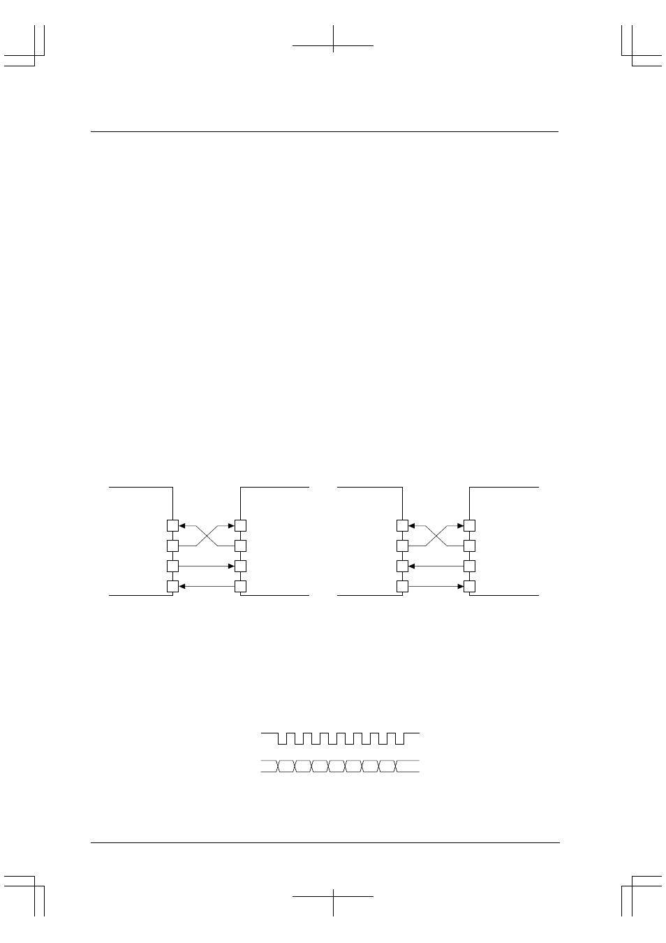
Figure 8.2 shows an example of how the input/output pins are connected in the clock-synchronized mode.
Data input
Data output
Clock input
Ready output
SINx
SOUTx
#SCLKx
#SRDYx
SINx
SOUTx
#SCLKx
#SRDYx
External
serial device
(1) Master mode
(2) Slave mode
S1C33
Data input
Data output
Clock output
Ready input
External
serial device
S1C33
Figure 8.2 Example of Connection in Clock-Synchronized Mode
Clock-synchronized transfer data format
In clock-synchronized transfers, the data format is fixed as shown below.
Data length: 8 bits
Start bit:
None
Stop bit:
None
Parity bit:
None
#SCLKx
Data
D0 D1 D2 D3 D4 D5 D6 D7
LSB
MSB
Figure 8.3 Clock-Synchronized Transfer Data Format
Serial data is transmitted and received starting with the LSB.
