I/o memory of i/o ports, Table 9.4 shows the control bits of the i/o ports – Epson S1C33210 User Manual
Page 368
III PERIPHERAL BLOCK: INPUT/OUTPUT PORTS
B-III-9-6
EPSON
S1C33210 FUNCTION PART
I/O Memory of I/O Ports
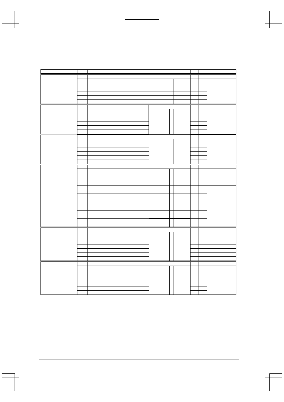
Table 9.4 shows the control bits of the I/O ports.
Table 9.4 Control Bits of I/O Ports
Name
Address
Register name
Bit
Function
Setting
Init.
R/W
Remarks
–
CFP05
CFP04
CFP03
CFP02
CFP01
CFP00
D7-6
D5
D4
D3
D2
D1
D0
Reserved
P05 function selection
P04 function selection
P03 function selection
P02 function selection
P01 function selection
P00 function selection
–
0
0
0
0
0
0
–
R/W
R/W
R/W
R/W
R/W
R/W
0 when being read.
Extended functions
(0x402DF)
00402D0
(B)
–
1 SOUT1
0 P05
1 SIN1
0 P04
1 #SRDY0
0 P03
1 #SCLK0
0 P02
1 SOUT0
0 P01
1 SIN0
0 P00
P0 function
select register
–
P05D
P04D
P03D
P02D
P01D
P00D
D7-6
D5
D4
D3
D2
D1
D0
reserved
P05 I/O port data
P04 I/O port data
P03 I/O port data
P02 I/O port data
P01 I/O port data
P00 I/O port data
–
0
0
0
0
0
0
–
R/W
R/W
R/W
R/W
R/W
R/W
0 when being read.
00402D1
(B)
–
High
0
1
Low
P0 I/O port data
register
–
IOC05
IOC04
IOC03
IOC02
IOC01
IOC00
D7-6
D5
D4
D3
D2
D1
D0
reserved
P05 I/O control
P04 I/O control
P03 I/O control
P02 I/O control
P01 I/O control
P00 I/O control
–
0
0
0
0
0
0
–
R/W
R/W
R/W
R/W
R/W
R/W
0 when being read.
00402D2
(B)
1 Output
0 Input
P0 I/O control
register
–
–
CFP16
CFP15
CFP14
CFP13
CFP12
CFP11
CFP10
D7
D6
D5
D4
D3
D2
D1
D0
reserved
P16 function selection 1
P15 function selection 1
P14 function selection
P13 function selection
P12 function selection
P11 function selection
P10 function selection
–
0
0
0
0
0
0
0
–
R/W
R/W
R/W
R/W
R/W
R/W
R/W
0 when being read.
Extended functions
(0x402DF)
00402D4
(B)
1 EXCL5
#DMAEND1
0 P16
1 EXCL4
#DMAEND0
0 P15
1 EXCL3
T8UF3
0 P13
1 EXCL2
T8UF2
0 P12
1 EXCL1
T8UF1
0 P11
1 EXCL0
T8UF0
0 P10
–
P1 function
select register
1 FOSC1
0 P14
–
P16D
P15D
P14D
P13D
P12D
P11D
P10D
D7
D6
D5
D4
D3
D2
D1
D0
reserved
P16 I/O port data
P15 I/O port data
P14 I/O port data
P13 I/O port data
P12 I/O port data
P11 I/O port data
P10 I/O port data
–
0
0
0
0
0
0
0
–
R/W
R/W
R/W
R/W
R/W
R/W
R/W
0 when being read.
00402D5
(B)
1 High
0 Low
–
P1 I/O port data
register
–
IOC16
IOC15
IOC14
IOC13
IOC12
IOC11
IOC10
D7
D6
D5
D4
D3
D2
D1
D0
reserved
P16 I/O control
P15 I/O control
P14 I/O control
P13 I/O control
P12 I/O control
P11 I/O control
P10 I/O control
–
0
0
0
0
0
0
0
–
R/W
R/W
R/W
R/W
R/W
R/W
R/W
0 when being read.
00402D6
(B)
1 Output
0 Input
–
P1 I/O control
register