Section 12 – serial peripheral interface (spi), 1 – spi transfer formats, Section 12 – Maxim Integrated DS4830 Optical Microcontroller User Manual
Page 99: Serial peripheral interface (spi), Spi transfer formats, Ds4830 user’s guide
DS4830 User’s Guide
99
SECTION 12
– SERIAL PERIPHERAL INTERFACE (SPI)
The DS4830 provides two independent Serial Peripheral Interfaces (SPI)
– one defined as SPI Master and SPI Slave.
Each SPI module of the DS4830 microcontroller provides an independent serial communication channel to communicate
synchronously with peripheral devices in a multiple master or multiple slave system. Each interface allows independent
access to a four-wire full-duplex serial bus that can be operated in either master mode or slave mode. The SPI
functionality must be enabled by setting the SPI Enable (SPIEN) bit of the SPI Control register to
‘1’. The maximum data
rate of the SPI interface is 1/2 the system clock frequency for master mode operation and 1/4 the system clock frequency
for slave mode operation.
Note: Even though SPI Master and SPI Slave interfaces are defined, each interface can operate as SPI Master or SPI
Slave or both.
The four external interface signals used by the SPI module are MOSI (Master Out Slave In), MISO (Master In Slave Out),
SPI Clock (SPICK), and Slave Select (SSEL).
SPI Status and Control Unit
SHIFT Register
15/7
15/7
Receive Data Buffer
0
0
SPIB
Writes
SPIB
Reads
MOSI
MISO
SPICK
SSEL
SPI Master
SPICN.MSTM = 1
SPIEN =
SPICN.0
SPI Status and Control Unit
SHIFT Register
15/7
15/7
Receive Data Buffer
0
0
SPIB
Writes
SPIB
Reads
MISO
MOSI
SPICK
SSEL
SPI Slave
SPICN.MSTM = 0
SPIEN =
SPICN.0
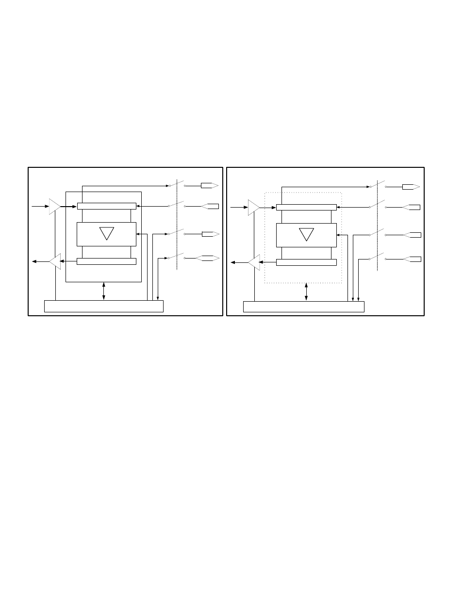
Figure 12-1
:
SPI Master and Slave Block Diagram
12.1
– Serial Peripheral Interface (SPI) Detailed Description
The block diagram Figure 12-1 shows the SPI external interface signals, control unit, read buffer, and single shift register
common to the transmit and receive data path for both the master and slave blocks. SPI can be viewed as a synchronous
serial I/O port that shifts data stream of variable length (8 or 16 bits) between peripheral devices. Data is shifted out of the
SPI through the programmable shift register which is formed by serially connecting the master’s shift register and a slave
shift register.
Each time that an SPI transfer completes, the received character is transferred to the read buffer, giving double buffering
on the receive side. The CPU has read/write access to the control unit and the SPI data buffer (SPIB). Writes to SPIB are
always directed to the shift register while reads always come from the receive data buffer. During an SPI transfer, data is
simultaneously transmitted and received. The serial clock signal (SPICK) synchronizes shifting and sampling of the bit
stream on the two serial data pins.
For both the master and the slave, data is shifted out of the shift register on one edge of SPICK and latched into the shift
register on the opposite SPICK clock edge. The master can initiate data transfer at any time since it controls the serial
clock. The slave select signal (SSEL) allows individual selection of slave SPI device in the network.
12.1.1
– SPI Transfer Formats
During an SPI transfer, data is simultaneously transmitted and received over two serial data lines with respect to a single
serial shift clock. The polarity and phase of the serial shift clock are the primary components in defining the SPI data
transfer format. The polarity of the serial clock corresponds to the idle logic state of the clock line and therefore also
defines which clock edge is the active edge. To define a serial shift clock signal that idles in a logic low state (active clock
edge = rising), the Clock Polarity Select (CKPOL; SPICF.0) bit should be configured to a 0, while setting CKPOL = 1 will
cause the shift clock to idle in a logic high state (active clock edge = falling). The phase of the serial clock selects which