Ds4830 user’s guide – Maxim Integrated DS4830 Optical Microcontroller User Manual
Page 106
DS4830 User’s Guide
106
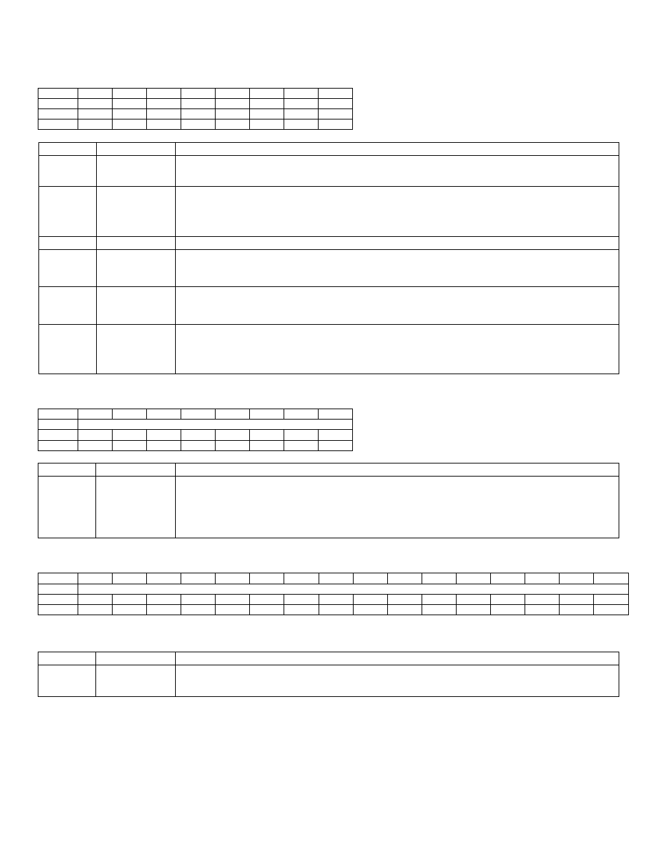
12.4.3.2
– SPI Configuration Register (SPICF_M)
SPICF_M Register Address: M5 [13h]
Bit
7
6
5
4
3
2
1
0
Name
ESPII
SAS
-
-
-
CHR
CKPHA
CKPOL
Reset
0
0
0
0
0
0
0
0
Access
rw
rw
r
r
r
rw
rw
rw
BIT
NAME
DESCRIPTION
7
ESPII
SPI Interrupt Enable. Se
tting this bit to ‘1’ enables the SPI interrupt when MODF, WCOL,
ROVR or SPIC flags are set. Clearing this bit to ‘0’ disables the SPI interrupt.
6
SAS
Slave Active Select.
In Master mode, this is used only when mode fault is enabled.
If SAS = 0, then mode fault is detected when active low is detected on MSPICS pin.
If SAS = 1, then mode fault is detected when active high is detected on MSPICS pin.
5:3
Reserved
Reserved, Read Returns 0.
2
CHR
Character Length Bit. The CHR bit determines the character length for an SPI transfer
cycle. A character can consist of 8 or 16 bits in length. When CHR bit is ‘0’, the character is
8 bits; when CHR is set to ‘1’, the character is 16 bits.
1
CKPHA
SPI Clock Phase Select. This bit is used with the CKPOL bit to determine the SPI transfer
format. When the CKPHA is set to
‘1’, the SPI will sample input data at an inactive edge.
When the CKPOL is cleared to 0, the SPI will sample input at an active edge.
0
CKPOL
SPI Clock Polarity Select. This bit is used with the CKPHA bit to determine the SPI
transfer format. When the CKPOL is set to
‘1’, the SPI uses the clock falling edge as
an active edge. When the CKPOL is cleared to 0, the SPI selects the clock rising edge as
an active edge.
12.4.3.3
– SPI Clock Register (SPICK_M)
SPICK_M Register Address: M5 [14h]
Bit
7
6
5
4
3
2
1
0
Name
SPICK_M[7:0]
Reset
0
0
0
0
0
0
0
0
Access
rw
rw
rw
rw
rw
rw
rw
rw
BIT
NAME
DESCRIPTION
7:0
SPICK_M[7:0] Clock Divide Ratio Bits. These bits select one of the 256 divide ratios (0 to 255) used for
the baud rate generator, with bit 7 as the most significant. The frequency of SPI baud rate
is calculated using the following equation:
SPI Baud Rate = ½ x System Clock / (SPICK[7:0] + 1)
12.4.3.4
– SPI Data Buffer Register (SPIB_M)
SPIB_M Register Address: M5 [04h]
Bit
15
14
13
12
11
10
9
8
7
6
5
4
3
2
1
0
Name
SPIB_M[15:0]
Reset
0
0
0
0
0
0
0
0
0
0
0
0
0
0
0
0
Access*
rw
rw
rw
rw
rw
rw
rw
rw
rw
rw
rw
rw
rw
rw
rw
rw
*Unrestricted read, write is allowed outside of a transfer cycle; when the STBY bit is set, write is blocked and will cause
write collision error.
BIT
NAME
DESCRIPTION
15:0
SPIB_M[15:0]
SPI Data Buffer Bits. Data for SPI is read from or written to this location. The serial
transmit and receive buffers are separate but both are addressed at this location.