2 – read register map command host-rom interaction, Read register map command host-rom interaction – Maxim Integrated DS4830 Optical Microcontroller User Manual
Page 162
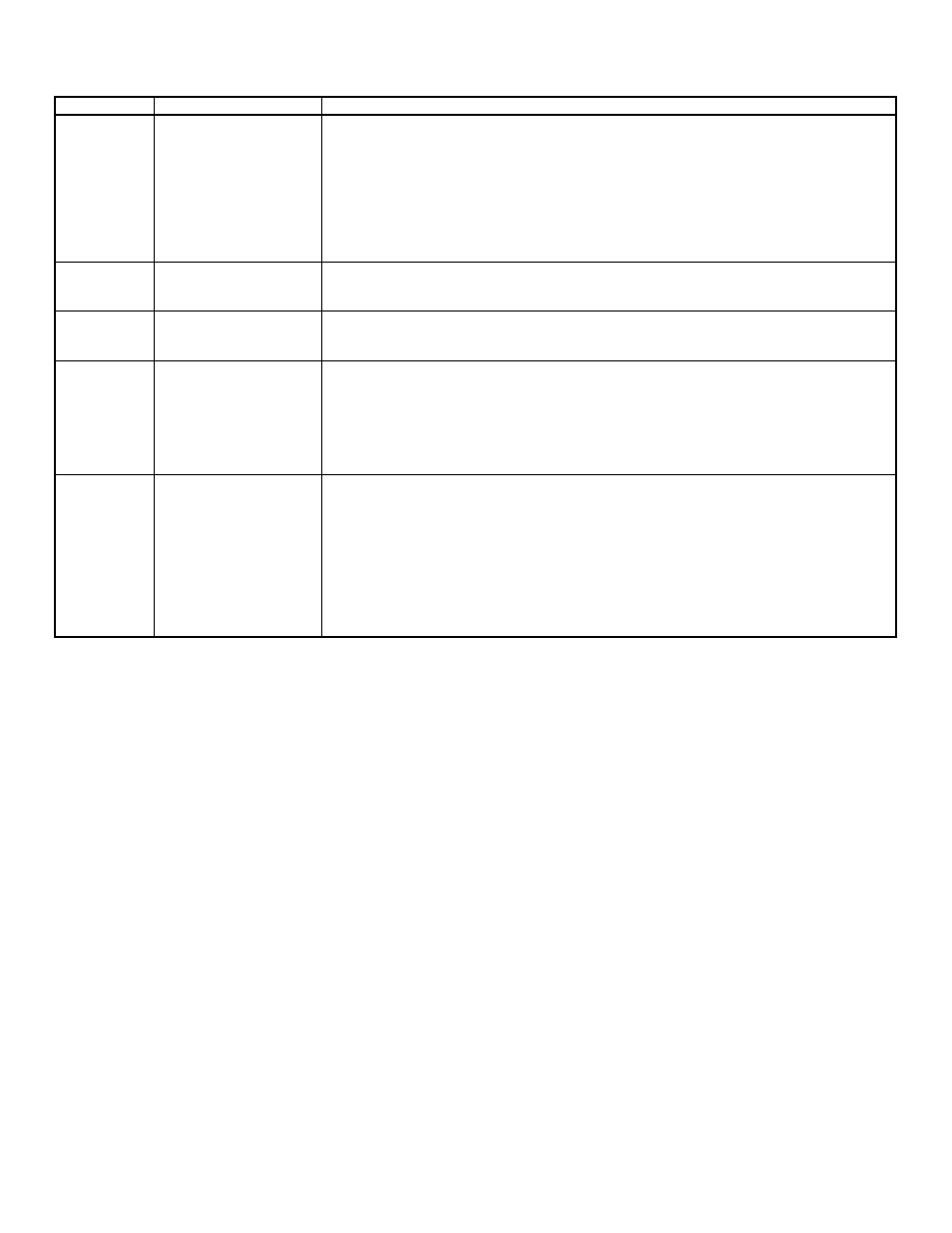
DS4830 User’s Guide
162
Op Code
Command
Operation
0010-0101
Write data memory
Write data to a selected data memory location. This command requires four follow-on
transfer cycles, two for the memory address and two for the data, starting with the LSB
address and ending with the MSB data.
The input address must be based memory map
when executing from utility ROM, as shown in Figure 2-4.
The address is moved to the
ICDA register and the data is moved to the ICDD register by the debug engine. This
information is directly accessible by the ROM code. At the completion of this command
period, the debug engine updates the CMD3:0 bits to 0101b and performs a jump to ROM
code at x8010h. The ROM Debug service routine will update the selected data memory
location according to the information received in the ICDA and ICDD registers.
0010-0110
Trace
Trace command. This command allows single stepping the CPU and requires no follow-on
transfer cycle. The trace operation is a ‘debug mode exit, one cycle CPU execution, debug
mode entry’ sequence.
0010-0111
Return
Return command. This command terminates the debug mode and returns the debug
engine to background mode. This allows the CPU to resume its normal operation at the
point where it has been last interrupted.
0010-1000
Unlock password
Unlock the password lock. This command requires 32 follow-on transfer cycles each
containing a byte value to be compared with the program memory password for the purpose
of clearing the PWL bit and granting access to protected debug and loader functions. When
this command is received, the debug engine updates the CMD3:0 bit to 1000b and performs
a jump to ROM code at x8010h. Data is loaded to the ICDB register when each byte of data
is received, beginning with the LSB of the least significant word first and end with the MSB
of the most significant word.
0010-1001
Read register
Read from a selected internal register. This command requires two follow-on transfer
cycles, starting with the LSB address and ending with the MSB address. The address is
moved to ICDA register by the debug engine. This information is directly accessible by the
ROM code. At the completion of this command period, the debug engine updates the
CMD3:0 bits to 1001b and performs a jump to ROM code at x8010h. The ROM Debug
service routine will always assume a 16-bit register length and return the requested data
LSB first.
Reading a register through the debug interface returns the value that was in that register
before the debugging engine was invoked. An exception to this rule is the SP register;
reading the SP register through the debug interface actually returns the value (SP+1).
21.2.2
– Read Register Map Command Host-ROM Interaction
A read register map command reads out data contents for all implemented system and peripheral registers. The host
does not specify a target register but instead should expect register data output in successive order, starting with the
lowest order register in register module 0. Data is loaded by the ROM to the 8-bit ICDB register and is output one byte per
transfer cycle. Thus, for a 16-bit register, two transfer cycles are necessary. The host initiates each transfer cycle to shift
out the data bytes and will find valid data output tagged with a debug-valid (status = 11b). At the end of each transfer
cycle, the debug engine clears the TXC flag to signal the ROM service routine that another byte may be loaded to ICDB.
The ROM service routine sets the TXC flag each time after loading data to the ICDB register. This process is repeated
until all registers have been read and output to the host. The host system recognizes the completion of the register read
when the status debug-idle is presented. This indicates that the debug engine is ready for another operation.
This command outputs all peripheral registers in the range M0[00h] to M5[17h], along with a fixed set of system registers.
The following formatting rules apply to the returned data:
All peripheral registers are output as 16 bits, least significant byte first. If the register is an 8-bit register, the top is
returned as 00h.
System registers are output as 8 bits or 16 bits, least significant byte first.
Registers I2CBUF_S, I2CBUF_M, SPIB_M, SPIB_S, QTDATA, PWMDATA and ADDATA are not read. Their
values are returned as 0000h.
Nonimplemented and reserved peripheral registers in the range M0[00h] to M5[17h] are represented as empty
word values in Table 21-4. These values should be ignored.
The first byte output by this command is the value 180 (B4h), which represents the number of words output for peripheral
register. There are a total of 216 words that are output by this command. Table 21-4 lists all of the registers output and
the order in which they are output.