Ds4830 user’s guide – Maxim Integrated DS4830 Optical Microcontroller User Manual
Page 57
DS4830 User’s Guide
57
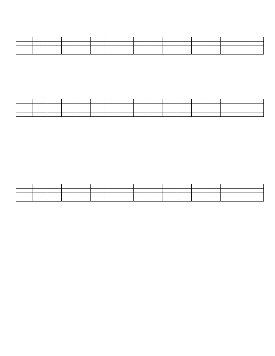
7.2.8
– ADC External Temperature Offset Register (TOEX)
Register Address: M1 [1Ah]
Bit
15
14
13
12
11
10
9
8
7
6
5
4
3
2
1
0
Name
S
S
S
S
2
8
2
7
2
6
2
5
2
4
2
3
2
2
2
1
2
0
2
-1
2
-2
2
-3
Reset
s
s
s
s
s
s
s
s
s
s
s
S
s
s
s
s
Access
rw
rw
rw
rw
rw
rw
rw
rw
rw
rw
rw
rw
rw
rw
rw
rw
s = special, initial value is dependent on trim settings
This register contains the temperature offset for the external temperature measurements. The default value of this
register is -273 (Kelvin to Celsius) plus any offset that was calibrated out at the factory. This offset is applied to the raw
data from the ADC prior to the value being stored into the data buffer. The final result stored in the data buffer will be
raw_adc + TOEX, where raw_adc is the converted temperature in Kelvin.
7.2.9
– ADC Voltage Offset Register (ADVOFF)
Register Address: M1 [19h]
Bit
15
14
13
12
11
10
9
8
7
6
5
4
3
2
1
0
Name
S
S
S
2
12
2
11
2
10
2
9
2
8
2
7
2
6
2
5
2
4
2
3
2
2
2
1
2
0
Reset
s
s
s
s
s
s
s
s
s
s
s
s
s
s
s
s
Access
rw
rw
rw
rw
rw
rw
rw
rw
rw
rw
rw
rw
rw
rw
rw
rw
s = special, initial value is dependent on trim settings
This register contains the ADC voltage offset for the voltage mode. This is calibrated for ADCG1 at the factory to cancel
out any offset that may be present in the ADC. The user can add or subtract any offset that they desire by altering this
register. This offset is applied to the raw data from the ADC prior to the value being stored into the data buffer. The value
stored in the data buffer will be raw_adc + ADVOFF, where raw_adc is the converted voltage without any offset
compensation.
7.2.10
– ADC Voltage Scale Trim Registers (ADCG1, ADCG2, ADCG3 and ADCG4)
ADCG1 Register Address: M1 [17h]
ADCG2 Register Address: M1 [18h]
ADCG3 Register Address: M1 [1Bh]
ADCG4 Register Address: M1 [1Ch]
Bit
15
14
13
12
11
10
9
8
7
6
5
4
3
2
1
0
Name
ADCG.15
ADCG.14
ADCG.13
ADCG.12
ADCG.11
ADCG.10
ADCG.9
ADCG.8
ADCG.7
ADCG.6
ADCG.5
ADCG.4
ADCG.3
ADCG.2
ADCG.1
ADCG.0
Reset
s
s
S
s
s
s
s
s
s
s
S
s
s
s
s
s
Access
rw
rw
rw
rw
rw
rw
rw
rw
rw
rw
rw
rw
rw
rw
rw
rw
s = special, initial value is dependent on trim settings
These registers are used to adjust the ADC full scale by changing the gain applied to the ADC reference (internal). These
registers are set at the factory to work with the internal reference. The internal reference voltage is set to 1.2V and cannot
be changed by the user.
These gain registers are provided so the ADC full scale can be adjusted to meet the needs of the targeted application.
Only bits ADCG[15:2] are used to adjust the full scale level. Some approximate settings are:
ADCGx = 32A8h: The full scale is ~1X the reference level
ADCGx = 1960h: The full scale is ~2X the reference level
ADCGx = 0B90h: The full scale is ~4X the reference level
ADCGx = 0328h: The full scale is ~6X the reference level
It is not recommended that a gain other than 1X, 2X, 4X or 6X be used. This is because the weightings of the ADCGx
[15:0] bits are non-linear. An application specific program needs to be developed that tests the ADC full scale for each
possible code setting until the proper full scale is achieved. It is recommended that the user not change ADCG1. The ADC
controller uses ADCG1 (not user selectable) for Sample and Hold.