Ds4830 user’s guide – Maxim Integrated DS4830 Optical Microcontroller User Manual
Page 121
DS4830 User’s Guide
121
PWM_SEL REG_SEL
Local Register Selected
0
0
Duty Cycle Register PWM Channel 0 (DCYC0)
0
1
PWM Configuration Register PWM Channel 0 (PWMCFG0)
0
2
Delay Setting Register for PWM Channel 0 (PWMDLY0)
1
0
Duty Cycle Register PWM Channel 1 (DCYC1)
1
1
PWM Configuration Register PWM Channel 1 (PWMCFG1)
1
2
Delay Setting Register for PWM Channel 1 (PWMDLY1)
2
0
Duty Cycle Register PWM Channel 2 (DCYC2)
2
1
PWM Configuration Register PWM Channel 2 (PWMCFG2)
2
2
Delay Setting Register for PWM Channel 2 (PWMDLY2)
3
0
Duty Cycle Register PWM Channel 3 (DCYC3)
3
1
PWM Configuration Register PWM Channel 3 (PWMCFG3)
3
2
Delay Setting Register for PWM Channel 3 (PWMDLY3)
4
0
Duty Cycle Register PWM Channel 4 (DCYC4)
4
1
PWM Configuration Register PWM Channel 4 (PWMCFG4)
4
2
Delay Setting Register for PWM Channel 4 (PWMDLY4)
5
0
Duty Cycle Register PWM Channel 5 (DCYC5)
5
1
PWM Configuration Register PWM Channel 5 (PWMCFG5)
5
2
Delay Setting Register for PWM Channel 5 (PWMDLY5)
6
0
Duty Cycle Register PWM Channel 6 (DCYC6)
6
1
PWM Configuration Register PWM Channel 6 (PWMCFG6)
6
2
Delay Setting Register for PWM Channel 6 (PWMDLY6)
7
0
Duty Cycle Register PWM Channel 7 (DCYC7)
7
1
PWM Configuration Register PWM Channel 7 (PWMCFG7)
7
2
Delay Setting Register for PWM Channel 7 (PWMDLY7)
8
0
Duty Cycle Register PWM Channel 8 (DCYC8)
8
1
PWM Configuration Register PWM Channel 8 (PWMCFG8)
8
2
Delay Setting Register for PWM Channel 8 (PWMDLY8)
9
0
Duty Cycle Register PWM Channel 9 (DCYC9)
9
1
PWM Configuration Register PWM Channel 9 (PWMCFG9)
9
2
Delay Setting Register for PWM Channel 9 (PWMDLY9)
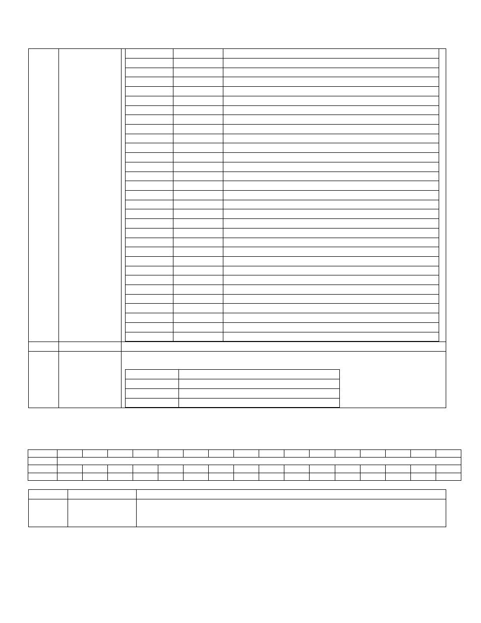
3:2
Reserved
Reserved. The user should write 0 to these bits.
1:0
REG_SEL[1:0]
Register Select. These bits are used to select one of three local registers of the selected
PWM channel (selected by PWM_SEL[3:0] bits).
REG_SEL
Local Register Selected
00b
Duty Cycle Register (DCYCn)
01b
PWM Configuration Register (PWMCFGn)
1xb
Delay Setting Register (PWMDLYn)
14.3.2
– PWM Data Register (PWMDATA Register)
PWMDATA Register Address: M5 [05h]
Bit
15
14
13
12
11
10
9
8
7
6
5
4
3
2
1
0
Name
PWMDATA[15:0]
Reset
0
0
0
0
0
0
0
0
0
0
0
0
0
0
0
0
Access
rw
rw
rw
rw
rw
rw
rw
rw
rw
rw
rw
rw
rw
rw
rw
rw
BIT
NAME
DESCRIPTION
15:0
PWMDATA[15:0] PWM Data. The PWM Data Register is used for configurations for various PWM
channels. It is used to read or write various PWM local registers which are pointed by
combinations of REG_SEL[1:0] and PWM_SEL[3:0] bits in the PWMCN register.
The PWMDATA Register is used to configure the local registers for each PWM channel. PWM channel is selected by
PWM_SEL[3:0] bits in the PWMCN register. Individual local registers for a channel are selected by REG_SEL[1:0] bits in
the PWMCN register. See below for the local register configurations