Section 13 – 3-wire, 1 – detailed description, 1 – operation – Maxim Integrated DS4830 Optical Microcontroller User Manual
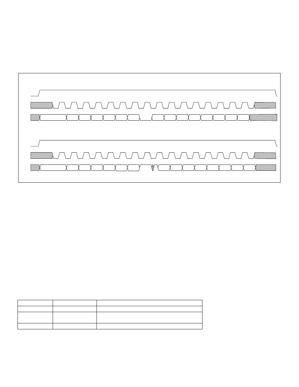
Page 110: Section 13, Wire, Detailed description, Operation, Ds4830 user’s guide, Figure 13-1: 3-wire write and read operation

DS4830 User’s Guide
110
SECTION 13
– 3-WIRE
The DS4830 has proprietary 3-Wire master interface for communication with MAXIM 3-wire laser drivers (which supports
MSB first 3-wire protocol). The 3-wire communication mode operates similar to SPI mode. However, in the 3-wire mode,
there is one bi-directional I/O instead of separate data in and data out signals. The 3-wire interface consists of the MCS,
MDIO and MCL. The 3-Wire Master interface reads data on the falling edge of MCL. During 3-Wire write operation the 3-
Wire master outputs the data on the falling edge of MCL.
MCS
MCL
1
2
3
4
5
6
7
8
A6
9
10
11
12
13
14
15
0
A5
A4
A3
A2
A1
RWN
D7
D6
D5
D4
D3
D2
D1
D0
1
2
3
4
5
6
7
8
A6
9
10
11
12
13
14
15
0
A5
A4
A3
A2
A1
RWN
D7
D6
D5
D4
D3
D2
D1
D0
WRITE MODE
READ MODE
A0
A0
MCS
MCL
MDIO
MDIO
Figure 13-1: 3-Wire Write and Read Operation
13.1
– Detailed Description
The DS4830 has a proprietary 3-Wire digital serial interface and it is designed to interface with Maxim 3-wire slave
devices (Laser drivers). The DS4830 acts as the 3-Wire master. It is a 3-pin interface consisting of MDIO a bidirectional
data line, MCL clock signal and MCS chip select output. Chip select is active high. The 3-Wire master initiates
communication by generating clock.
By default, 3-Wire Chip select is enabled and it is automatically controlled by 3-Wire interface during the communication.
The DS4830 3-Wire interface supports byte mode data transfer. The 3-Wire Control Register (TWR) is used to control and
configure the 3-Wire interface. The 3-Wire interface provides 8 user selectable MCL clock frequencies. The 3-Wire
communication is enabled by setting the TWEN bit to ‘1’ in the TWR register and MCS goes to low. Data transfer is
initiated on next core clock after writing to the Data and Address Register (DADDR).
13.1.1
– Operation
The DS4830 3-wire master supports 8 user configurable communication clock frequencies. These are selected by writing
to the TWCP [2:0] bits in the TWR register. Each 3-Wire packet consists of 16-bits (15-bit address/data, 1-bit RWN). Refer
Table 13-1 for 3-Wire Data Packet.
Table 13-1. 3-Wire Data Packet
Bit Number
Name
Description
15 to 9
ADDR (Address)
7-bit Internal Register Address (3-Wire Slave)
8
RWN
0 - write
1
– read
7 to 0
DATA
8-bit Read or Write Data
The 3-Wire interface is enabled when the TWEN bit in the TWR
register is set to ‘1’. Using the DADDR register 3-Wire
write (RWN = 0) and read (RWN = 1) operations are performed. The 3-Wire master supports 7-bit read or write address
and 8-bit data. Write to the DADDR register automatically starts the data transfer and the 3-Wire interface sets BUSY flag
to ‘1’. The BUSY flag is reset to ‘0’ when the data transfer is completed.
