9 – receiving data, Receiving data, Ds4830 user’s guide – Maxim Integrated DS4830 Optical Microcontroller User Manual
Page 81: Transmitting byte receiving byte, Transmitting slave address
DS4830 User’s Guide
81
I2CNACKI =
ACKNOWLEDGE
Transmit I2CBUF_M[7:0]
I2CBUF_M[0] I2CMODE
I2CBUSY=1
I2CTXI=1
I2CBUSY=0
Write to
I2CBUF_M
RECEIVE
ACKNOWLEDGE
Transmitting
Byte
Receiving
Byte
I2CNACKI =
ACKNOWLEDGE
Transmit Shift
Register Byte,
MSB First
N
Y
I2CBUSY=1
8 Bits
Transmit?
I2CTXI=1
I2CBUSY=0
Write to
I2CBUF_M
Receive a Bit into
Shift Register
MSB first
N
Y
I2CBUSY=1
8 Bits
Received?
Load Shift
Register into
I2CBUF_M
I2CRXI=1
Send
I2CACK
Y
N
I2CROI=1
Receiver
Full
?
First SCL
Rising Edge
Generated
I2CBUSY=0
RECEIVE
ACKNOWLEDGE
Transmitting
Slave Address
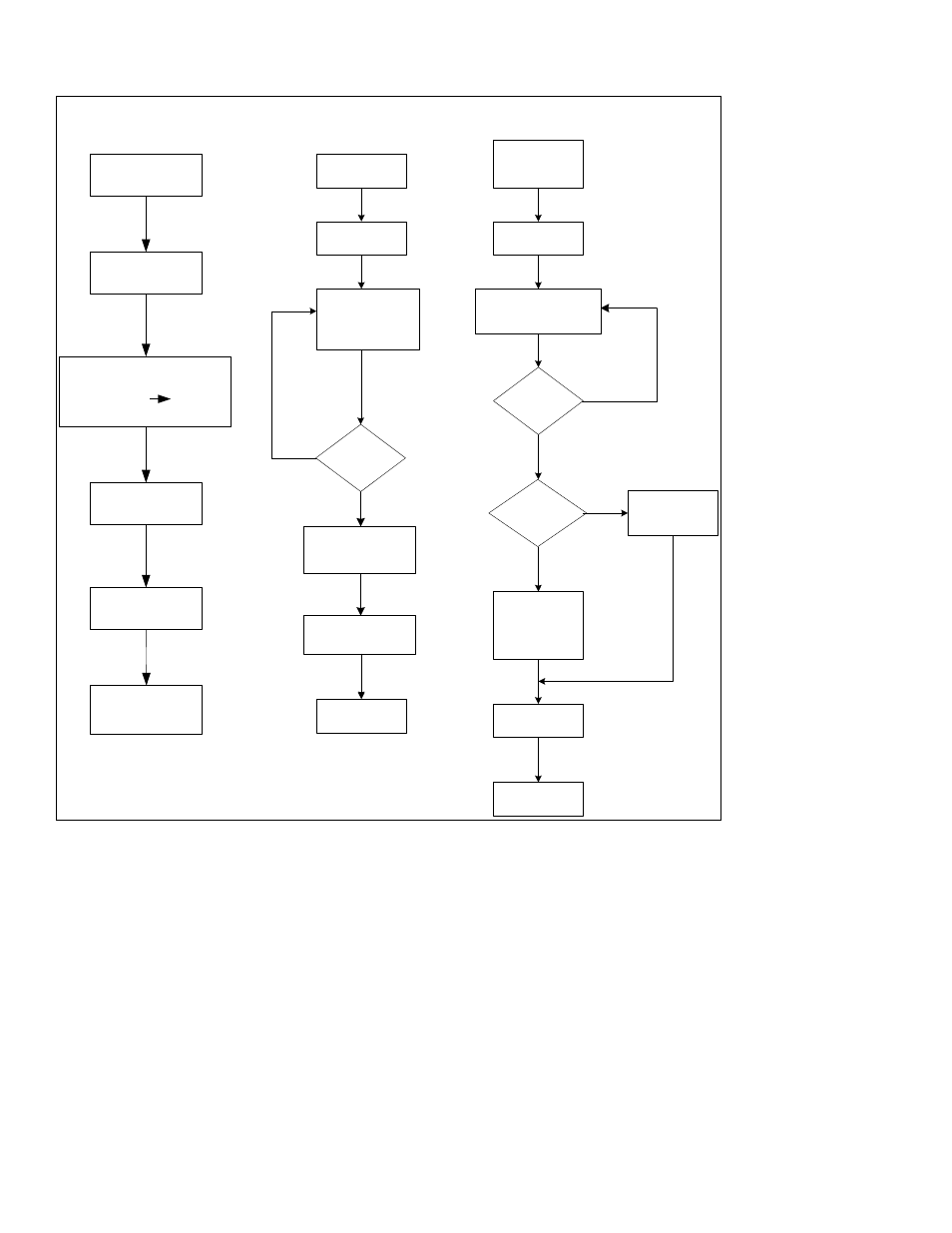
Figure 10-5: Master I
2
C Data Flow
10.1.9
– Receiving Data
The DS4830 I
2
C Master Controller enters data reception mode after transmitting a slave address with the R/W bit
(I2CMODE) set to a 1. The steps of data reception are shown in Figure 10-5. After transmitting the slave address, the
master controller will switch to receiver mode and automatically begin outputting SCL clock pulses and shifting in data
from SDA.
When receiving data, the DS4830 I
2
C master controller uses a double buffer consisting of the I2CBUF_M register and the
shift register. This allows the I
2
C module to continue receiving data while the previous data byte is being processed.
When a full byte of data (8 bits) has been received by the I
2
C master controller, the master must send an
acknowledgement to the slave. This occurs during the 9
th
clock cycle when the value in I2CACK is transmitted to the
slave.
After a complete byte (8 bits) of data is received, the I
2
C master controller will attempt to copy the received data from the
shift register to I2CBUF_M. There are two possible results from the I
2
C master controller
’s attempt to copy the shift
register to I2CBUF_M.