3 – pwm output register descriptions, Pwm output register descriptions, Ds4830 user’s guide – Maxim Integrated DS4830 Optical Microcontroller User Manual
Page 120
DS4830 User’s Guide
120
14.2.3.1
– PWM DELAY with PWMSYNC SFR
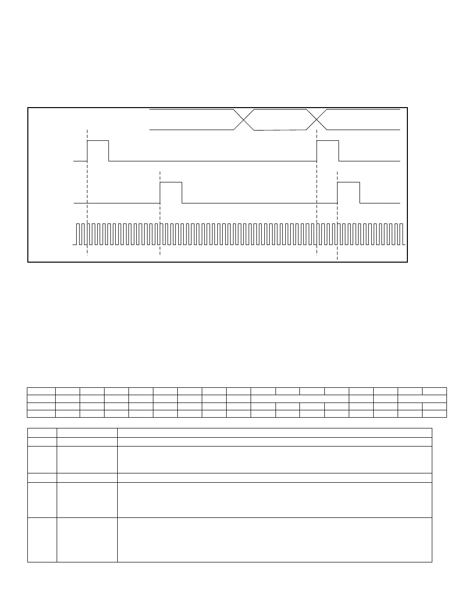
The PWM channels to be synchronized must have the same configurations (Resolution, Pulse Spreading option, Clock source
etc.). The Delays on the two channels can be different. After the synchronization, the programmed delay is maintained as shown
in Figure 14-7.
PWMSYNC = 00h
PWMSYNC = 03h
PWMSYNC = 00h
PWM1
PWM0
Core Clock
Figure 14-7: PWM output synchronization with 4 clock delay
14.3
– PWM Output Register Descriptions
The DS4830 PWM controller has 3 SFRs. These are PWM Control Register PWMCN, PWM Data Register PWMDATA
and PWM Synchronization Register PWMSYNC. The PWMCN configures and controls the various PWM operations. The
PWMDATA register configures various PWM configurations and the PWMSYNC is used in PWM synchronization
operation. The PWMCN, PWMDATA and PWMSYNC registers are cleared on POR only.
14.3.1
– PWM Control Register (PWMCN)
The PWMCN is used to setup and start the PWM Output. To avoid undesired operation, the user should NOT modify the
“Reserved” bits in the PWMCN registers.
PWMCN Register Address: M5 [06h]
Bit
15
14
13
12
11
10
9
8
7
6
5
4
3
2
1
0
Name
-
-
-
M_EN
-
-
-
UPDATE
PWM_SEL[3:0]
-
-
REG_SEL[1:0]
Reset
0
0
0
0
0
0
0
0
0
0
0
0
0
0
0
0
Access
r
r
r
rw
r
r
r
rw
rw
rw
rw
rw
r
r
rw
rw
BIT
NAME
DESCRIPTION
15:13
-
Reserved. The user should write 0 to these bits.
12
M_EN
Master Enable. This is the master enable bit for all PWM channels. All the PWM channels
will be enabled only after this bit is set to ‘1’. This bit should be set to ‘1’, after configuring
all local registers of all the required PWM channels.
11:9
-
Reserved. The user should write 0 to these bits.
8
UPDATE
Update.
When this bit is set to ‘1’, the duty cycle of all PWM channels are updated
simultaneously. Writing a new value in the Duty Cycle register will not reflect in the PWM
output until UPDATE is set to ‘1’. Once set, this bit will automatically clear after one core
clock.
7:4
PWM_SEL[3:0] PWM Channel Select. These bits select one of the 10 PWM channels for read or write to
its local registers. These bits are used with REG_SEL[1:0] and provide access to 30 PWM
local registers (3 local registers per channel). PWM_SEL auto increments after each read
or write operation to PWMDATA register.