Ds4830 user’s guide – Maxim Integrated DS4830 Optical Microcontroller User Manual
Page 55
DS4830 User’s Guide
55
6
ADALIGN
ADC Data Alignment Select. This bit selects the ADC data alignment mode. Setting this bit to
‘1’ returns ADC data left aligned in ADDATA [15:2] with ADDATA[1:0] zero padded. Clearing
this bit to ‘0’ returns ADC data in right aligned format in ADDATA[13:0] with ADDATA[15:14]
sign-extended by ADDATA[13].
5
ADDIFF
ADC Differential Mode Select. This bit selects the ADC conversion mode. When this bit is set
to ‘1’, the ADC conversion is in differential mode. When this bit is cleared to ‘0’, the ADC
conversion is performed in single-ended mode. During single ended mode, the sample is
measured between ADC Channel and ground.
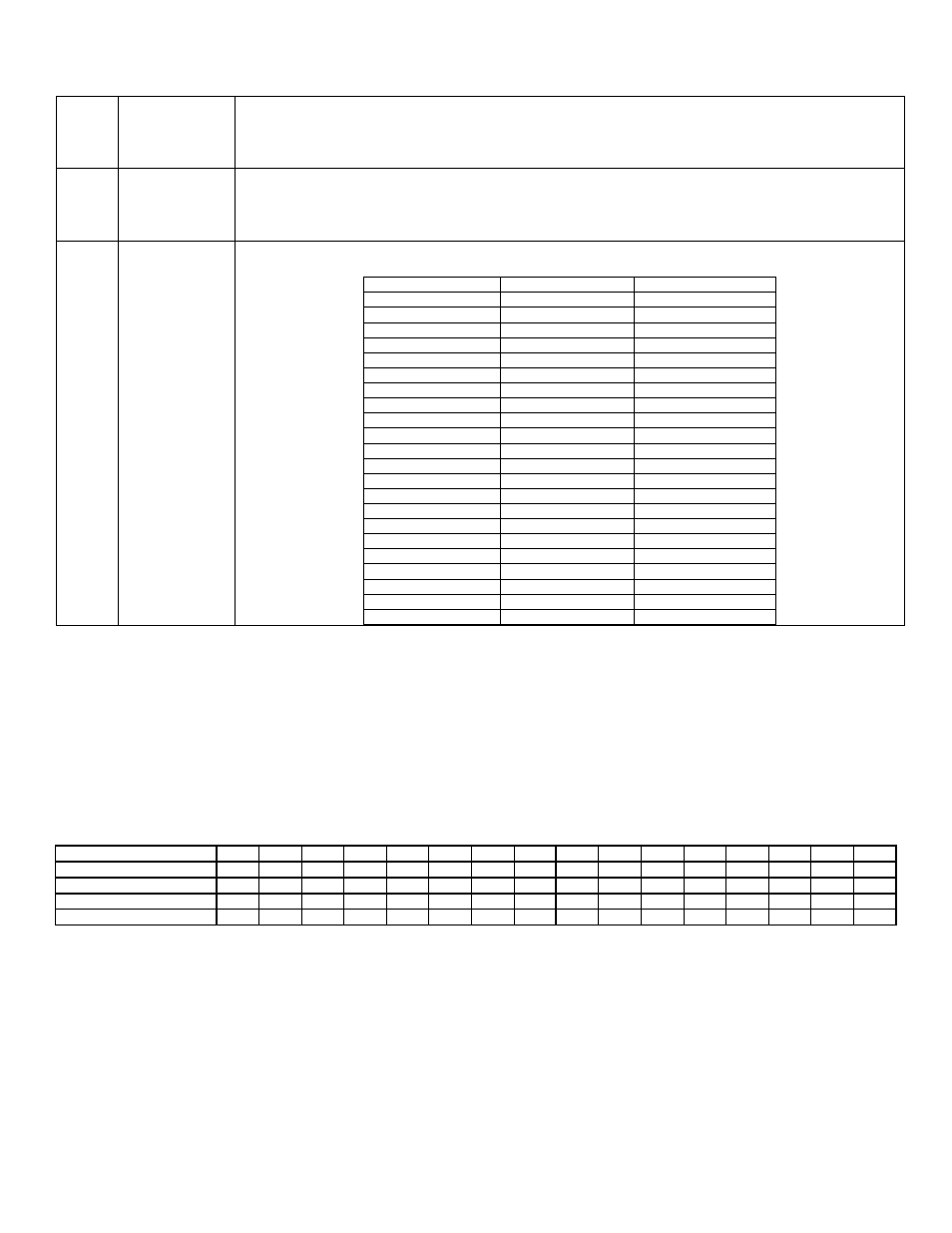
4:0
ADCH[4:0]
ADC Channel Select. These bits select the input channel source for configuration of ADC
conversion.
ADCH [4:0]
ADDIFF = 0
ADDIFF=1
00000
ADC-S0
ADC-D0P- ADC-D0N
00001
ADC-S1
ADC-D1P- ADC-D1N
00010
ADC-S2
ADC-D2P- ADC-D2N
00011
ADC-S3
ADC-D3P- ADC-D3N
00100
ADC-S4
ADC-D4P- ADC-D4N
00101
ADC-S5
ADC-D5P- ADC-D5N
00110
ADC-S6
ADC-D6P- ADC-D6N
00111
ADC-S7
ADC-D7P- ADC-D7N
01000
ADC-S8
NOT VALID
01001
ADC-S9
NOT VALID
01010
ADC-S10
NOT VALID
01011
ADC-S11
NOT VALID
01100
ADC-S12
NOT VALID
01101
ADC-S13
NOT VALID
01110
ADC-S14
NOT VALID
01111
ADC-S15
NOT VALID
10000
ADC-REFINA
ADC-REFINA
10001
ADC-REFINB
ADC-REFINB
10010
VDD
VDD
10011
DAC_INT_REF
DAC_INT_REF
10100-
11000
NOT VALID
NOT VALID
11001
ADC OFFSET
ADC OFFSET
7.2.5.2
– ADC Data Buffer (ADDATA when ADCFG = 0)
When ADCFG = 0, reading from the ADDATA register will read the ADC results stored in one of the 25 data buffers. The
ADIDX[4:0] bits point to the data buffer to be read. Reading ADDATA register returns the 14-bits (13-bits plus a sign bit) of
ADC conversion data from the selected data buffer memory. The ADIDX[4:0] bits will automatically increment after a read
of ADDATA. This allows multiple reads of ADDATA to access consecutive data buffer locations without needing to change
the ADIDX[4:0] bits. The data buffers will be reset to 0 on all forms of reset and are not writable by the user.
The data that is read from the ADC Buffer may be from either a temperature or voltage conversion. Also, the data may be
right or left aligned. Table 7-4 shows the returned bit weighting for each type of conversion.
Table 7-4. Voltage Data (ADC and Sample and Hold) and Temperature Bit weighting with alignment option
Bit
15
14
13
12
11
10
9
8
7
6
5
4
3
2
1
0
Temperature Right Aligned
S
S
S
2
8
2
7
2
6
2
5
2
4
2
3
2
2
2
1
2
0
2
-1
2
-2
2
-3
2
-4
Temperature Left Aligned
S
2
8
2
7
2
6
2
5
2
4
2
3
2
2
2
1
2
0
2
-1
2
-2
2
-3
2
-4
0
0
Voltage Right Aligned
S
S
S
2
12
2
11
2
10
2
9
2
8
2
7
2
6
2
5
2
4
2
3
2
2
2
1
2
0
Voltage Left Aligned
S
2
12
2
11
2
10
2
9
2
8
2
7
2
6
2
5
2
4
2
3
2
2
2
1
2
0
0
0
The ADC controller produces temperature, sample and hold and ADC data reading in the
2’s complement format.