Section 7 – analog-to-digital converter (adc), 1 – detailed description, 1 – adc controller – Maxim Integrated DS4830 Optical Microcontroller User Manual
Page 46: Section 7, Analog-to-digital converter (adc), Detailed description, Adc controller, Ds4830 user’s guide
DS4830 User’s Guide
46
SECTION 7
– ANALOG-TO-DIGITAL CONVERTER (ADC)
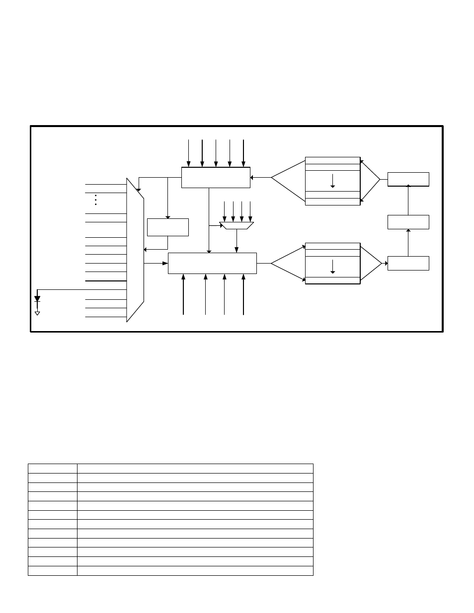
The DS4830 provides a 13-bit analog-to-digital converter (ADC) with 26-input MUX. As shown in Figure 7-1, the MUX
selects the ADC input from 16 external channels, DAC external references at REFINA and REFINB, VDD, DAC Internal
Reference, Internal Die Temperature, External Remote Diode temperatures at GP8-GP9 and GP10-GP11, Sample and
Hold at GP2-GP3 and GP12-GP13 and ADC Internal Offset. The ADC external channels can operate in differential
voltage mode or in single-ended voltage mode. GP8-GP9 and GP10-GP11 channels can be configured to measure the
temperature of an external diode. An internal channel is used exclusively to measure the die temperature.
13-BIT ADC CORE
ADC-S0
ADC-S1
ADC-S14
ADC-S15
A
N
A
L
O
G
M
U
X
V
O
L
T
A
G
E
O
F
F
S
E
T
(A
D
V
O
F
F
)
T
E
M
P
E
R
A
T
U
R
E
O
F
F
S
E
T
(
T
O
E
X
)
INTERNAL DIE TEMPERATURE
Current Source
For Temperature
Measurement
T
E
M
P
E
R
A
T
U
R
E
S
C
A
L
E
(
E
T
S
)
ADC SEQUENCER
A
D
S
T
A
R
T
A
D
E
N
D
A
D
C
O
N
V
A
D
C
O
N
T
A
D
C
G
1
A
D
C
G
4
ADGAIN
IN
T
E
R
N
A
L
R
E
F
E
R
E
N
C
E
CONFIGURATION[0]
CONFIGURATION[19]
CONFIGURATION[1]
DATA BUFFER[0]
DATA BUFFER[24]
DATA BUFFER[1]
ADCFG=1
ADIDX[4:0]
ADCFG=0
ADIDX[4:0]
ADDATA
A
D
C
G
3
A
D
C
G
2
REFINA
REFINB
DAC INT REF
VDD
EXT1 DIODE
EXT0 DIODE
SH0
SH1
Internal Offset
N
U
M
_
S
M
P
CONFIGURATION[23]
Figure 7-1: ADC Functional Block Diagram
7.1
– Detailed Description
7.1.1
– ADC Controller
The ADC controller is the digital interface block between CPU and the ADC. It provides all necessary controls to the ADC
and the CPU interface. The ADC controller provides 25 buffers (0-24) for various configurations and data buffers. By
default, the ADC conversion result is placed at the location shown in Table 7-1. The user can override the default buffers
and define alternate locations in the ADC Data and Configuration register (ADDATA) during configuration by settling the
LOC_OV
R bit to ‘1’ in the ADC Control register (ADCN). The internal and remote diode temperature sensors and Sample
and Hold (S/H) use fixed data buffer locations. The ADC internal offset does not have any data buffer and its
measurement is performed with location override enable. Table 7-1 has the default configuration and data buffer
locations.
Table 7-1. ADC Configuration and Data buffers
Data buffer Configuration / Data Buffer Selection
0-15
External Channels (0-15 in Single Ended or 0-7 in Differential)
16
REFINA
17
REFINB
18
VDD (Supply Voltage)
19
DAC Internal Reference
20
External Diode Temperature 1
21
External Diode Temperature 0
22
Internal Die Temperature
23
Sample and Hold 0
24
Sample and Hold 1
0-24 (Any)
ADC Internal Offset (with Location Override)