Ds4830 user’s guide – Maxim Integrated DS4830 Optical Microcontroller User Manual
Page 167
DS4830 User’s Guide
167
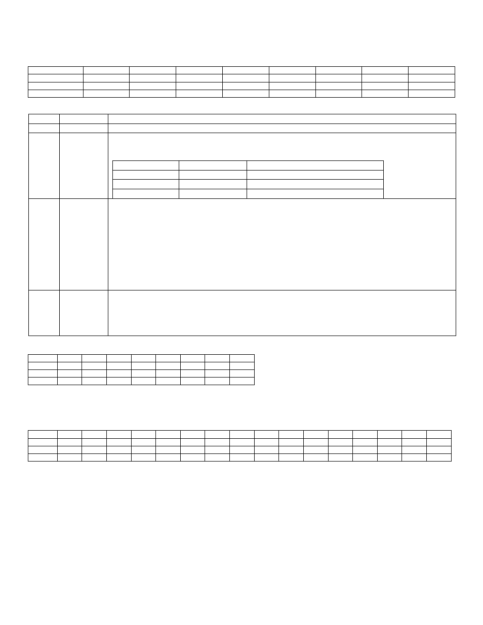
21.3.4
– In-Circuit Debug Flag Register (ICDF, M2[1Bh])
Bit
7
6
5
4
3
2
1
0
Name
-
-
-
-
PSS1
PSS0
JTAG_SPE
TXC
Reset
0
0
0
0
0
0
0
0
Access
r
r
r
r
rw
rw
rw
rw
r = read, s = special
BIT
NAME
DESCRIPTION
7:4
Reserved
Reserved. Do not write to these bits.
3:2
PSS[1:0]
Programming Source Select Bits [1:0]. These bits are used to select a programming interface
during In-System programming when JTAG_SPE is set to 1, otherwise, the logic values of these
bits have no meaning:
PSS1
PSS0
Interface/Action
0
0
JTAG
0
1
I2C
1
x
Exit Loader
1
JTAG_SPE System Program Enable. The JTAG_SPE bit is used for In-System programming support and its
logical state, when read by the CPU, always reflects the logical-OR of the JTAG_SPE bit that is
write accessible by the CPU and the SPE bit of the System Programming Buffer (SPB) Register
in the TAP Module (which is accessible via JTAG). The logical state of this bit determines the
program flow after a reset. When it is set to logic 1, In-System programming will be executed by
the Utility ROM. When it is cleared to 0, execution will be transferred to user code if I2C
bootloading is not required. This bit allows read/write access by the CPU and is cleared to 0 only
on a power-on reset or Test-Logic-Reset. The JTAG SPE bit will be cleared by hardware when
the ROD bit is set. CPU writes to the JTAG_SPE bit (0 or 1) will result in clearing of the PSS[1:0]
bits.
0
TXC
Serial Transfer Complete. This bit is set by hardware at the end of a transfer cycle at the TAP
communication link. The TXC bit helps the debug engine to recognize host requests, either
command or data. This bit is normally set by ROM code to signify or request the sending or
receiving of data. The TXC bit is cleared by the debug engine once set. CPU writes to the TXC
bit results in clearing of the PSS[1:0] bits.
21.3.5
– In-Circuit Debug Buffer Register (ICDB, M2[1Ch])
Bit
7
6
5
4
3
2
1
0
Name
ICDB.7
ICDB.6
ICDB.5
ICDB.4
ICDB.3
ICDB.2
ICDB.1
ICDB.0
Reset
0
0
0
0
0
0
0
0
Access
rw
rw
rw
rw
rw
rw
rw
rw
This register serves as the parallel holding buffer for the debug shift register of the TAP. Data is read from or written to
ICDB for serial communication between the debug routines and the external host.
21.3.6
– In-Circuit Debug Address Register (ICDA, M2[1Dh])
Bit
15
14
13
12
11
10
9
8
7
6
5
4
3
2
1
0
Name
ICDA.15
ICDA.14
ICDA.13
ICDA.12
ICDA.11
ICDA.10
ICDA.9
ICDA.8
ICDA.7
ICDA.6
ICDA.5
ICDA.4
ICDA.3
ICDA.2
ICDA.1
ICDA.0
Reset
0
0
0
0
0
0
0
0
0
0
0
0
0
0
0
0
Access
r
r
r
r
r
r
r
r
r
r
r
r
r
r
r
r
This register is used by the debug engine to store addresses so that ROM code can view that information. This register is
also used by the debug engine as a mask register to mask out don’t care bits in the ICDD register when BP5 is used as a
register breakpoint. When a bit in this register is set to 1, the corresponding bit location in the ICDD register will be
compared to the data being written to the destination register to determine if a break should be generated. When a bit in
this register is cleared, the corresponding bit in the ICDD re
gister becomes a don’t care and is not compared against the
data being written. When all bits in this register are cleared, any updated data pattern will cause a break when the BP5
register matches the destination register address of the current instruction.