Ds4830 user’s guide – Maxim Integrated DS4830 Optical Microcontroller User Manual
Page 26
DS4830 User’s Guide
26
3.5 Interrupt Mask Register (IMR, 8h[6h])
Initialization: This register is cleared to 00h on all forms of reset.
Access: Unrestricted read/write access.
Bit
Name
Function
7
IMS
Interrupt Mask for System Modules
6
Reserved
Reserved. All reads return 0.
5
IM5
Interrupt Mask for Register Module 5
4
IM4
Interrupt Mask for Register Module 4
3
IM3
Interrupt Mask for Register Module 3
2
IM2
Interrupt Mask for Register Module 2
1
IM1
Interrupt Mask for Register Module 1
0
IM0
Interrupt Mask for Register Module 0
The first six bits in this register are interrupt mask bits for modules 0 to 5, one bit per module. The eighth bit, IMS, serves
as a mask for any system module interrupt sources. Setting a mask bit allows the enabled interrupt sources for the
associated module or system (for the case of IMS) to generate interrupt requests. Clearing the mask bit effectively
disables all interrupt sources associated with that specific module or all system interrupt sources (for the case of IMS).
The interrupt mask register is intended to facilitate user-definable interrupt prioritization.
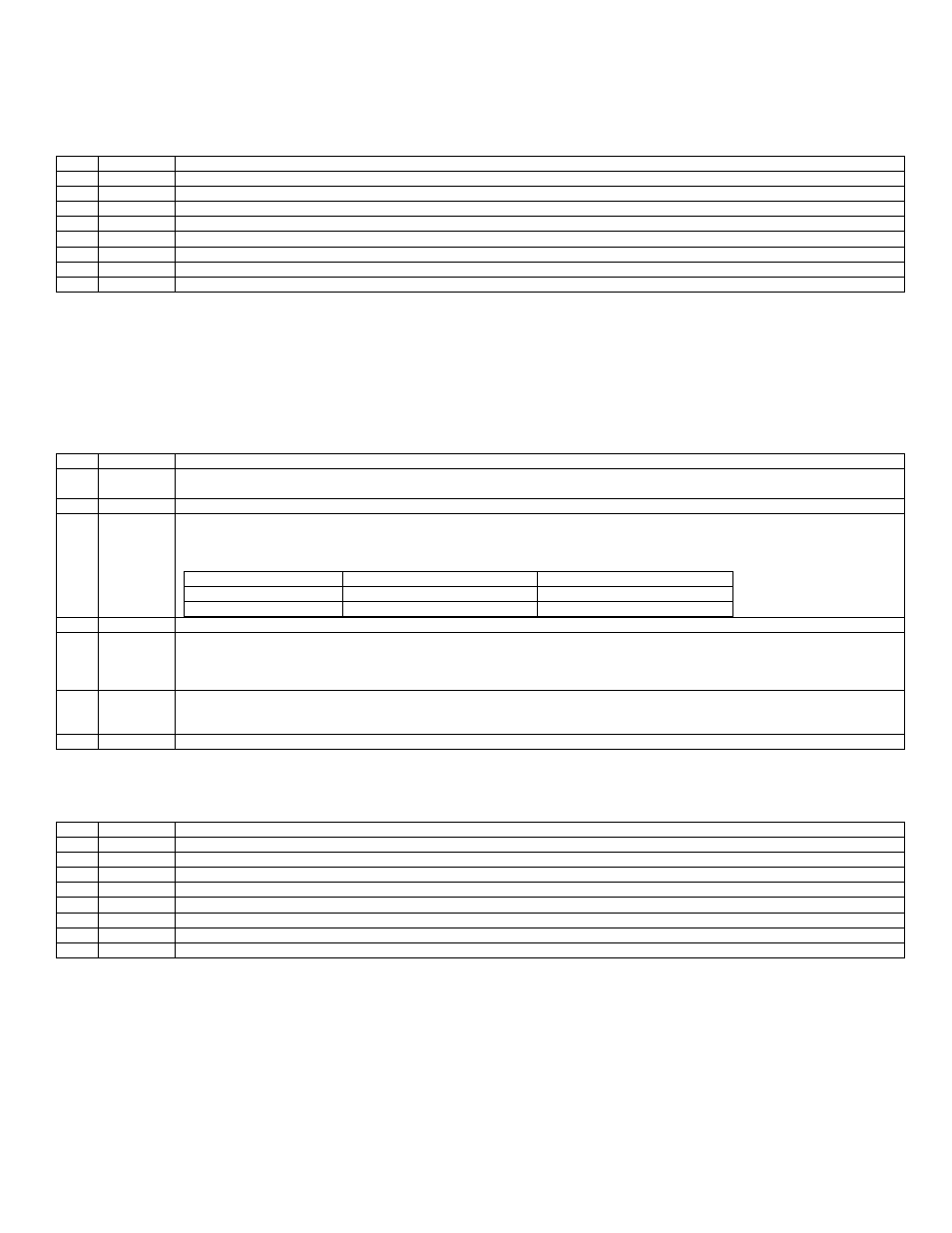
3.6 System Control Register (SC, 8h[8h])
Initialization: This register is reset to 1000 00s0b on all reset. Bit 1 (PWL) is set to 1 on a power-on reset only.
Access: Unrestricted read/write access.
Bit
Name
Function
7
TAP
Test Access Port (JTAG) Enable. This bit controls whether the Test Access Port special-function pins are enabled. The TAP
defaults to being enabled. Clearing this bit to 0 disables the TAP special function pins.
6:5
Reserved
Reserved. All reads return 0.
4
CDA0
Code Data Access Bit 0.
The CDA0 bit is used to logically map the flash memory pages to the data space for read/write access. The logical data memory
addresses of the flash depend on whether execution is from Utility ROM or SRAM. The CDA0 bit is not needed if data memory is
accessed in word mode.
CDA0
Byte Mode Active Page
Word Mode Active Page
0
P0
P0 and P1
1
P1
P0 and P1
3
Reserved
Reserved. All reads return 0.
2
ROD
ROM Operation Done. This bit is used to signify completion of a ROM operation sequence to the control units. This allows the
Debug engine to determine the status of a ROM sequence. Setting this bit to logic 1 causes an internal system reset if the JTAG
SPE bit is also set. Setting the ROD bit will clear the JTAG SPE and I2C_SPE bits if set. The ROD bit will be automatically
cleared by hardware once the control unit acknowledges the done indication.
1
PWL
Password Lock. This bit defaults to 1 on a power-on reset. When this bit is 1, it requires a 32-byte password to be matched with
the password in the program space before allowing access to the password protected in-circuit debug or bootstrap loader ROM
routines. Clearing this bit to 0 disables the password protection for these ROM routines.
0
Reserved
Reserved. All reads return 0.
3.7 Interrupt Identification Register (IIR, 8h[Bh])
Initialization: This register is cleared to 00h on all forms of reset.
Access: Read only.
Bit
Name
Function
7
IIS
Interrupt Identifier Flag for System Modules
6
Reserved
Reserved. All reads return 0.
5
II5
Interrupt Identifier Flag for Register Module 5
4
II4
Interrupt Identifier Flag for Register Module 4
3
II3
Interrupt Identifier Flag for Register Module 3
2
II2
Interrupt Identifier Flag for Register Module 2
1
II1
Interrupt Identifier Flag for Register Module 1
0
II0
Interrupt Identifier Flag for Register Module 0
The first six bits in this register indicate interrupts pending in modules 0 to 5, one bit per module. The eighth bit, IIS,
indicates a pending system interrupt, such as from the watchdog timer. The interrupt pending flags will be set only for
enabled interrupt sources waiting for service. The interrupt pending flag will be cleared when the pending interrupt
sources within that module are disabled or when the interrupt flags are cleared by software