2 – individual pwm channel operation, 1 – duty cycle register (dcycn), Individual pwm channel operation – Maxim Integrated DS4830 Optical Microcontroller User Manual
Page 115: Duty cycle register (dcycn)

DS4830 User’s Guide
115
14.2
– Individual PWM Channel Operation
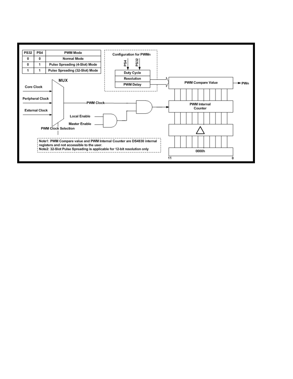
Figure 14-3: Block diagram of one PWM channel.
The DS4830 has 10 PWMs which can provide up to 12 bits of resolution on each channel. Each channel can be
independently enabled or disabled. Each PWMs is configured using 3 Local Registers (for a total of 30 Local Registers for
programming the 10 PWMs)
As explained above the PWMCN SFR points to a particular PWM channel. The local registers are then programmed by
writing data to the PWMDATA SFR. The Local Register are selected based on the REG_SEL bits in the PWMCN SFR
(See Table 14-1)
Details for programming of
the Local Registers are in the “PWM Register Descriptions” section.
14.2.1
– Duty Cycle Register (DCYCn)
This register controls the Duty cycle of the PWM Channel. The number of bits used to program the Duty Cycle depends
on the resolution programmed in the PWMCFG register. For 12 bits of resolution, the Duty cycle is the lower 12 bits of the
PWMDATA register. However if only 7 bits of resolution is selected, only the lower 7 bits are used to control the Duty
Cycle of the corresponding PWM Channel.
To achieve a particular duty cycle, the PWM output level is set to high and the internal counter starts counting from 0000h.
The PWM output remains high till the PWM count is equal to the value in the DCYC register. The PWM controller sets the
PWM output to low for the remaining clock counts for the selected resolution. One such cycle represents one PWM frame
and repeats until the PWM is disabled.
For example, when 9-bits of resolution is selected and the DCYC register is written to 128, the PWM controller sets the
output high for the first 128 counts of PWM clock and sets output low for the remaining 384 PWM clock counts (2
9
= 512
–
128 = 384). The PWM frame in this case is 512 clock cycles. The PWM output frequency depends upon the selected
clock source in the PWMCFG register. Figure 14-4 illustrates this example.
