4 – dr-scan sequence, 3 – communication via tap, Dr-scan sequence – Maxim Integrated DS4830 Optical Microcontroller User Manual
Page 152: Communication via tap
DS4830 User’s Guide
152
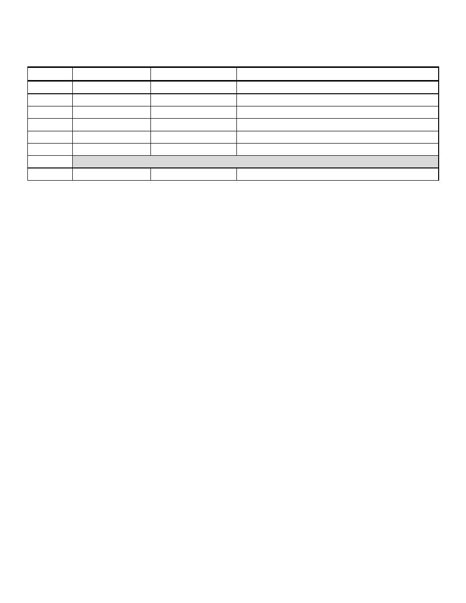
Table 20-3 - Instruction Register (IR2:0) Encodings
IR2:0
Instruction
Function
Serial Data Shift Register Selection
000
Extest
No operation
Unchanged. Retain previous selection
001
Sample/Preload
No operation
Unchanged. Retain previous selection
010
Debug
In-circuit debug mode
10-bit shift register
011
By-pass
No operation (default)
1-bit shift register
100
System Programming
Bootstrap function
3-bit shift register
101
By-pass
No operation (default)
1-bit shift register
110
Reserved
111
By-pass
No operation (default)
1-bit shift register
The Extest (IR2:0 = 000b) and Sample/Preload (IR2:0 = 001b) instructions are mandated by the JTAG standard, however,
the DS4830 does not intend to make practical use of these instructions. Hence, these instructions are treated as no
operations but may be entered into the instruction register without affecting the on-chip system logic or pins and does not
change the existing serial data register selection between TDI and TDO.
The By-pass (IR2:0 = 011b, 101b, or 111b) instruction is also mandated by the JTAG standard. The By-pass instruction is
fully implemented by the DS4830 to provide a minimum length serial data path between the TDI and the TDO pins. This is
accomplished by providing a single cell bypass shift register. When the instruction register is updated with the By-pass
instruction, a single bypass register bit is connected serially between TDI and TDO in the Shift-DR state. The instruction
register automatically defaults to the By-pass instruction when the TAP is in the Test-Logic-Reset state. The By-pass
instruction has no effect on the operation of the on-chip system logic.
The Debug (IR2:0 = 010b) and System Programming (IR2:0 = 100b) instructions are private instructions which are
intended solely for in-circuit debug and in-system programming operations respectively. If the instruction register is
updated with the Debug instruction, a 10-bit serial shift register is formed between the TDI and TDO pins in the Shift-DR
state. If the System Programming instruction is entered into the instruction register (IR2:0), a 3-bit serial data shift register
is formed between the TDI and TDO pins in the Shift-DR state.
Instruction register (IR2:0) settings other than those listed and described above are reserved for internal use. As can be
seen in Figure 20-2, the instruction register serves to select the length of the serial data register between TDI and TDO
during the Shift-DR state.
20.2.4
– DR-Scan Sequence
Once the instruction register has been configured to a desired state (mode), transactions are performed via a data buffer
register associated with that mode. These data transactions are executed serially in a manner analogous to the process
used to load the instruction register and are grouped in the TAP Controller state sequence starting from the Select-DR-
Scan state. In the TAP controller state sequence, the Shift-DR state allows internal data to be shifted out through the TDO
pin while the external data is shifted in simultaneously via the TDI pin. Once a complete data pattern is shifted in, input
data can be latched into the parallel buffer of the selected register on the falling edge of TCK in the Update-DR state. On
the same TCK falling edge, in the Update-DR state, the internal parallel buffer is loaded to the data shift register for
output. This Shift-DR/Update-DR process serves as the basis for passing information between the external host and the
DS4830. These data register transactions occur in the data register portion of the TAP controller state sequence diagram
and have no effect on the instruction register.
20.3
– Communication via TAP
The TAP controller is in Test-Logic-Reset state after a power-on-reset. During this initial state, the instruction register
contains By-pass instruction and the serial path defined between the TDI and TDO pins for the Shift-DR state is the 1-bit
bypass register. All TAP signals (TCK, TMS, TDI, and TDO) default to being weakly pulled high internally on any reset.
The TAP controller will remain in the Test-Logic-Reset state as long as TMS is held high. The TCK and TMS signals may
be manipulated by the host to transition to other TAP states. The TAP controller will remain in a given state whenever
TCK is held low.