2 – program memory mapping, 3 – data memory access, Program memory mapping – Maxim Integrated DS4830 Optical Microcontroller User Manual
Page 15: Data memory access

DS4830 User’s Guide
15
2.4.2
– Program Memory Mapping
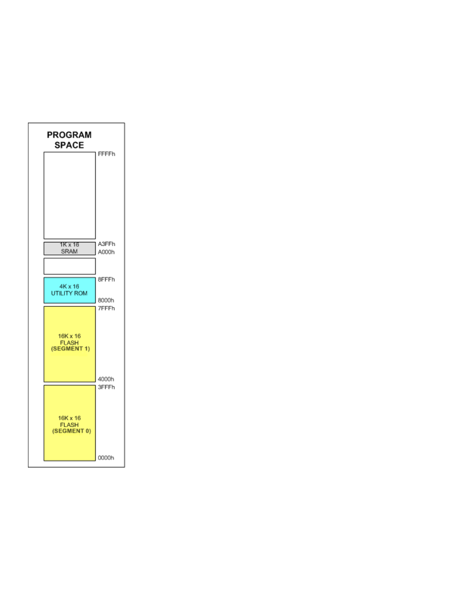
The DS4830’s mapping of the three memory segments (flash, SRAM, and utility ROM) as program memory is shown in
Figure 2-2. The mapping of memory segments into program space is always the same. When referring to memory as
program memory, all addresses are given as word addresses. The 32KWord flash memory segment is located at
memory location 0000h through 7FFFh and is logically divided into two pages, each containing 16KWords. The utility
ROM is located from location 8000h through 8FFFh, followed by the SRAM memory segment at location A000h through
A3FFh. The user code reset vector, which is the first instruction of user program code that is executed, is located at flash
memory address 0000h. User program code should always begin at this address.
Figure 2-2: Program Memory Mapping
2.4.3
– Data Memory Access
Data memory mapping and access control are handled by the memory management unit (MMU). Read/write access to
data memory can be in word or in byte mode. The DS4830 provides three pointers that can be used for indirect
accessing of data memory. The DS4830 has two data pointers (@DPn) and one frame pointer (@BP[OFFS]). These
pointers are implemented as registers that can be directly accessed by user software. A data memory access requires
only one system clock period.
2.4.3.1
– Data Pointers
To access data memory, the data pointers are used as one of the operands in a MOVE instruction. If the data pointer is
used as a source, the core performs a load operation that reads data from the memory location addressed by the data
