Section 8 – sample and hold, 1 – detailed description, 1 – operation – Maxim Integrated DS4830 Optical Microcontroller User Manual
Page 60: Section 8, Sample and hold, Detailed description, Operation, Ds4830 user’s guide
DS4830 User’s Guide
60
SECTION 8
– SAMPLE AND HOLD
The DS4830 has two independent, but identical, Sample and Hold differential channels. Sample and Hold 0 (S/H0) is on
GP2-GP3 and Sample and Hold 1 (S/H1) is on GP12-GP13. The sample and hold function can be configured for internal
or external triggering. Each sample and hold has a dedicated pin for external trigger.
Sampling
Control
A
N
A
L
O
G
M
U
X
Input
Discharge
Control
S/H Circuit
Current
Source
SHEN*
ADC
E
x
te
rn
a
l
C
lo
c
k
P
e
ri
p
h
e
ra
l
C
lo
c
k
Cs
Cs
*SHEN can be internal or external (SHEN0 or SHEN1)
SHP
SHN
Cp
Cp
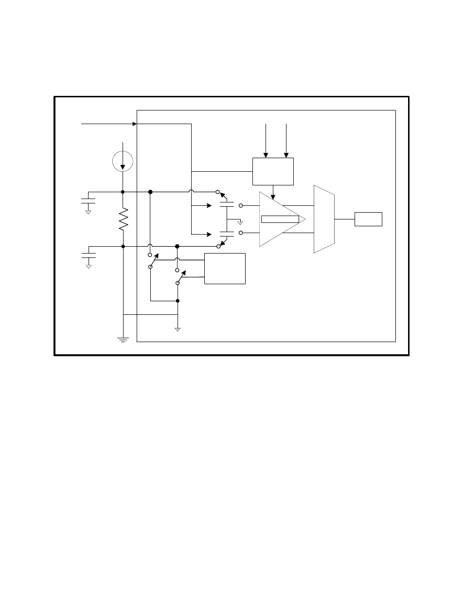
Figure 8-1: Sample and Hold Functional Block Diagram
8.1
– Detailed Description
As shown in figure 8-1, each Sample and Hold consists of fully differential sampling capacitors (C
s
), control logic and a
differential output buffer. The sample and hold also contains a charge injection nulling circuit. Additionally, it has a
discharge circuit to discharge parasitic capacitance on the input node and the sample capacitor before it starts sampling.
The input voltage is sampled using 5pF capacitor on the positive input and another 5pF capacitor on the negative input.
The negative input pin is used to reduce ground offset and noise. The capacitors are connected to the input when sample
trigger signal SHEN (either internal or external) is high. During high period of sample pulse, the sample and hold performs
sampling which ends at negative edge of the sample pulse SHEN. In addition to the sampling capacitors, the input pins
also have parasitic capacitance. When the sample and hold is configured for internal triggering, the sample pulse is
internally generated by the sample and hold hardware.
8.1.1
– Operation
When the SHEN signal goes high, the sample and hold capacitors are connected to the sample and hold input pins (GPx)
for sampling of the input signal. The minimum sample time for should be 300nSec for proper sampling. When the SHEN
signal goes low, the sampling is stopped and voltage stored at sampling capacitors are converted by the ADC controller.
See Figure 8-2 for Sample and Hold Timings. Each Sample and Hold can be independently enabled by setting their
respective enable bit in the Sample and Hold Control Register (SHCN). The sample and hold has two modes of operation
“Single Mode” and “Dual Mode”.