Table 3-3. watchdog timeout period selection -19, Table 3-4. system register map -19, Maxq family user’s guide – Maxim Integrated MAXQ Family User Manual
Page 44: Table 3-3. watchdog timeout period selection, Table 3-4. system register map
3-19
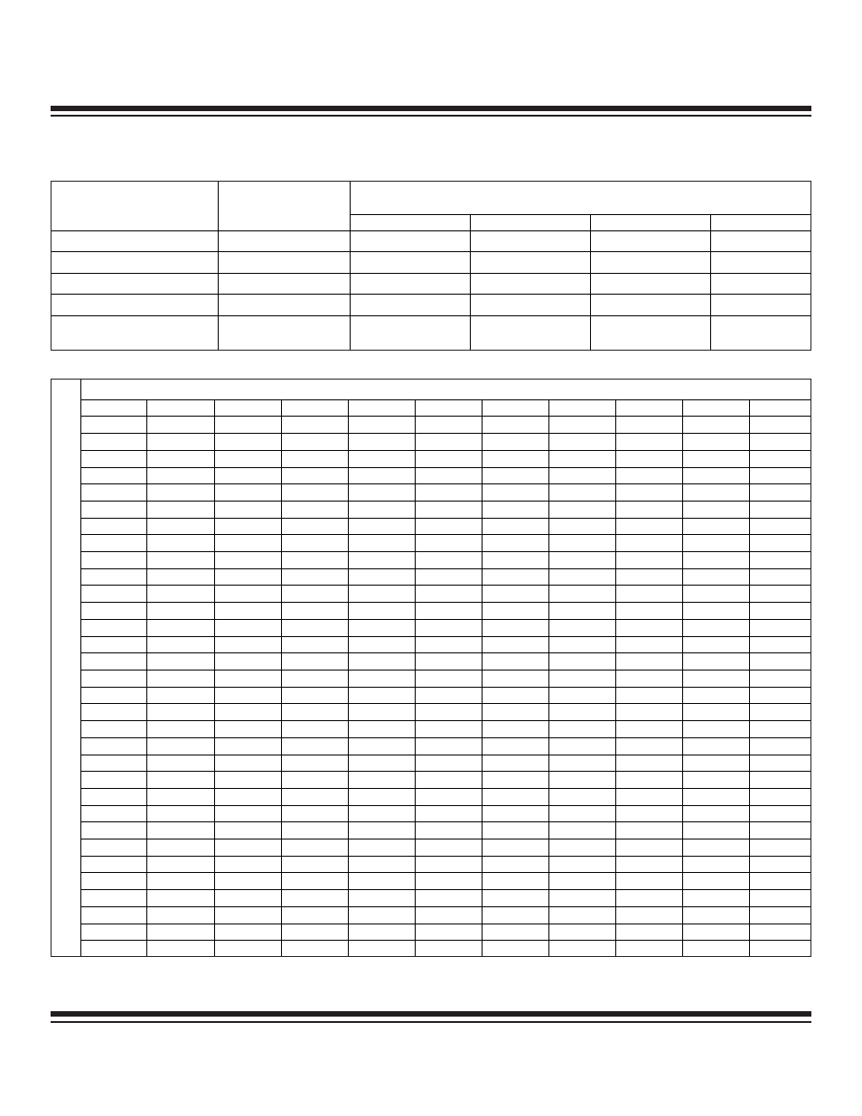
Table 3-3. Watchdog Timeout Period Selection
WATCHDOG TIMEOUT
(IN NUMBER OF OSCILLATOR CLOCKS)
SYSTEM CLOCK MODE
SYSTEM CLOCK
SELECT BITS PMME,
CD1, CD0
WD1:0 = 00b
WD1:0 = 01b
WD1:0 = 10b
WD1:0 = 11b
Divide by 1 (default)
000
2
12
2
15
2
18
2
21
Divide by 2
001
2
13
2
16
2
19
2
22
Divide by 4
010
2
14
2
17
2
20
2
23
Divide by 8
011
2
15
2
18
2
21
2
24
Power Management Mode
(Divide by 256)
1xx
2
20
2
23
2
26
2
29
Note: Registers in italics are read-only. Registers in bold are 16-bit (except A[n], Acc, A[AP] for MAXQ10). Registers with indexes 8h and higher can only be
accessed as destinations by using the prefix register. Similarly, registers with indexes 10h and higher can only be accessed as sources through the prefix regis-
ter. All undefined or unused indexes (indicated by an em-dash ‘—‘) are either used for op code implementation or reserved for future expansion, and should not
be accessed explicitly. Accessing these locations as registers can have deterministic effects, but the effects will probably not be the intended ones.
Table 3-4. System Register Map
MODULE SPECIFIER
6h
7h
8h
9h
Ah
Bh
Ch
Dh
Eh
Fh
0h
—
—
AP
A[0]
Acc
PFX[0]
IP
—
—
—
1h
—
—
APC
A[1]
A[AP]
PFX[1]
—
SP
—
—
2h
—
—
—
A[2]
—
PFX[2]
—
IV
—
—
3h
—
—
—
A[3]
—
PFX[3]
—
—
OFFS
DP[0]
4h
—
—
PSF
A[4]
—
PFX[4]
—
—
DPC
—
5h
—
—
IC
A[5]
—
PFX[5]
—
—
GR
—
6h
—
—
IMR
A[6]
—
PFX[6]
—
LC[0]
GRL
—
7h
—
—
—
A[7]
—
PFX[7]
—
LC[1]
BP
DP[1]
8h
—
—
SC
A[8]
—
—
—
—
GRS
—
9h
—
—
—
A[9]
—
—
—
—
GRH
—
Ah
—
—
—
A[10]
—
—
—
—
GRXL
—
Bh
—
—
IIR
A[11]
—
—
—
—
FP
—
Ch
—
—
—
A[12]
—
—
—
—
—
—
Dh
—
—
—
A[13]
—
—
—
—
—
—
Eh
—
—
CKCN
A[14]
—
—
—
—
—
—
Fh
—
—
WDCN
A[15]
—
—
—
—
—
—
10h
—
—
—
—
—
—
—
—
—
—
11h
—
—
—
—
—
—
—
—
—
—
12h
—
—
—
—
—
—
—
—
—
—
13h
—
—
—
—
—
—
—
—
—
—
14h
—
—
—
—
—
—
—
—
—
—
15h
—
—
—
—
—
—
—
—
—
—
16h
—
—
—
—
—
—
—
—
—
—
17h
—
—
—
—
—
—
—
—
—
—
18h
—
—
—
—
—
—
—
—
—
—
19h
—
—
—
—
—
—
—
—
—
—
1Ah
—
—
—
—
—
—
—
—
—
—
1Bh
—
—
—
—
—
—
—
—
—
—
1Ch
—
—
—
—
—
—
—
—
—
—
1Dh
—
—
—
—
—
—
—
—
—
—
1Eh
—
—
—
—
—
—
—
—
—
—
1Fh
—
—
—
—
—
—
—
—
—
—
REGISTER
INDEX
WITHIN
MODULE
MAXQ Family User’s Guide
Maxim Integrated