7 clock generation, 7 clock generation -13, Figure 2-7. maxq clock sources -13 – Maxim Integrated MAXQ Family User Manual
Page 18: Maxq family user’s guide
2-13
- Physical program memory pages (P0, P1, P2, P3) are logically mapped into data space based upon the memory segment
currently being used for execution, selection of byte/word access mode, and CDA1:0 bit settings (described under Pseudo Von
Neumann Memory Map and Pseudo Von Neumann Memory Access.)
• Data memory
- Access can be either word or byte.
- All 16 data pointer address bits are significant in either access mode (word or byte.)
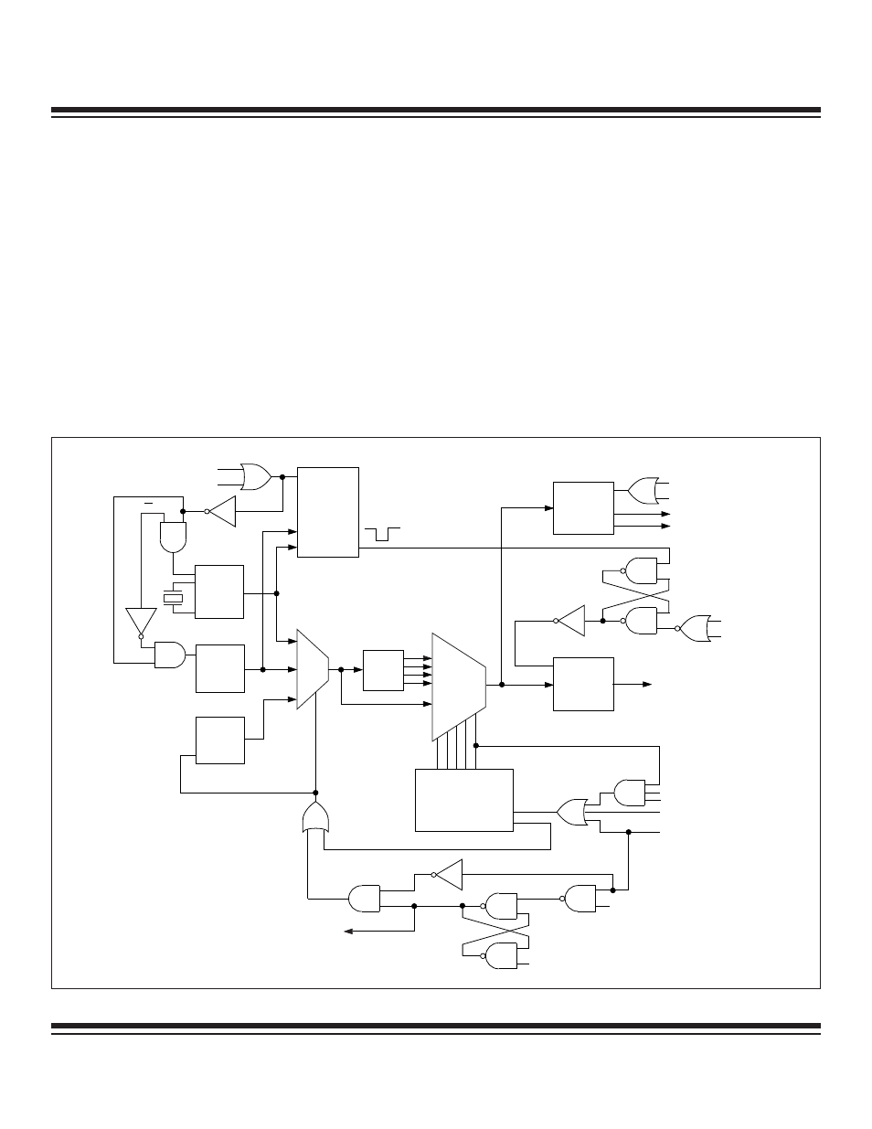
2.7 Clock Generation
All functional modules in the MAXQ are synchronized to a single system clock. The internal clock circuitry generates the system clock
from one of four possible sources:
• Internal ring oscillator
• Internal oscillator, using an external crystal or resonator
• Internal relaxation oscillator, using an external RC
• External clock signal
MAXQ
GLITCH-FREE
MUX
GLITCH-FREE
MUX
DIV
1
DIV
2
DIV
4
DIV
8
PMM
CLOCK
DIVIDER
SELECTOR
DEFAULT
RING SELECT
WATCHDOG
TIMER
RESET DOG
RWT
RESET
POWER-ON
RESET
STOP
XT/RC
STOP
POWER-ON
RESET
SWB
INTERRUPT/SERIAL PORT
RESET
STOP
RGSL
XDOG DONE
RGMD
WATCHDOG RESET
CLOCK
GENERATION
SYSTEM CLOCK
ENABLE
WATCHDOG INTERRUPT
RC
OSCILLATOR
ENABLE
RING OSC
ENABLE
HF
CRYSTAL
ENABLE
XDOG
STARTUP
TIMER
OSC IN
RESET
XDOG DONE
RC IN
Figure 2-7. MAXQ Clock Sources
MAXQ Family User’s Guide
Maxim Integrated