Figure 11-1. spi block diagram -2, Maxq family user’s guide – Maxim Integrated MAXQ Family User Manual
Page 114
11-2
MAXQ Family User’s Guide
SECTION 11: SERIAL PERIPHERAL INTERFACE (SPI) MODULE
The serial peripheral interface (SPI) module of the MAXQ microcontroller provides an independent serial communication channel to
communicate synchronously with peripheral devices in a multiple master or multiple slave system. The interface allows access to a
four-wire full-duplex serial bus that can be operated in either master mode or slave mode. The SPI functionality must be enabled by
setting the SPI Enable (SPIEN) bit of the SPI Control register to logic 1. The maximum data rate of the SPI interface is 1/2 the system
clock frequency for master mode operation and 1/8 the system clock frequency for slave mode operation. The four external interface
signals used by the SPI module are MISO, MOSI, SPICK, and SSEL. The function of each of these signals is as follows:
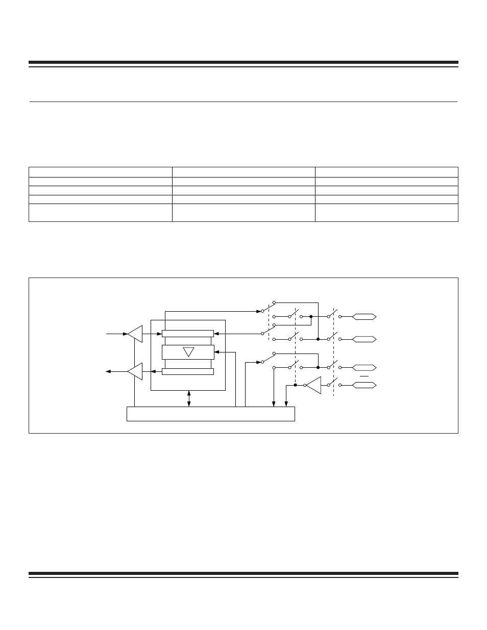
The block diagram in Figure 11-1 shows the SPI external interface signals, control unit, read buffer, and single shift register common
to the transmit and receive data path. Each time that an SPI transfer completes, the received character is transferred to the read buffer,
giving double buffering on the receive side. The CPU has read/write access to the control unit and the SPI data buffer (SPIB). Writes
to SPIB are always directed to the shift register while reads always come from the receive holding buffer.
EXTERNAL PIN SIGNAL
MASTER MODE USE
SLAVE MODE USE
MISO: Master In, Slave Out
Input to serial shift register
Output from serial shift register when selected
MOSI: Master Out, Slave In
Ouput from serial shift register
Input to serial shift register when selected
SPICK: SPI Clock
Serial shift clock sourced to slave device(s)
Serial shift clock from an external master
SSEL: Slave Select
(Optional) Mode fault-detection input if enabled
(MODFE = 1)
Slave select input
SPIEN =
SPICN.0
MSTM = SPICN.1
SHIFT REGISTER
MOSI
SPIB WRITES
RECEIVE DATA
BUFFER
SPIB READS
0
0
1
15/7
15/7
MISO
0
1
SPI STATUS & CONTROL UNIT
0
SPICK
1
0
SSEL
Figure 11-1. SPI Block Diagram
Maxim Integrated