1 instruction decoding, 1 instruction decoding -4, Figure 2-2. instruction word format -4 – Maxim Integrated MAXQ Family User Manual
Page 9: Maxq family user’s guide
2-4
MAXQ Family User’s Guide
Memory access from the MAXQ is based on a Harvard architecture with separate address spaces for program and data memory. The
simple instruction set and transport-triggered architecture allow the MAXQ to run in a nonpipelined execution mode where each instruc-
tion can be fetched from memory, decoded, and executed in a single clock cycle. Data memory is accessed through one of three data
pointer registers. Two of these data pointers, DP[0] and DP[1], are stand-alone 16-bit pointers. The third data pointer, FP, is composed
of a 16-bit base pointer (BP) and an 8-bit offset register (OFFS). All three pointers support post-increment/decrement functionality for
read operations and pre-increment/decrement for write operations. For the Frame Pointer (FP=BP[Offs]), the increment/decrement
operation is executed on the OFFS register and does not affect the base pointer (BP). Stack functionality is provided by dedicated
memory with a 16-bit width and a typical depth of 8 (although this varies dependent upon the MAXQ product). An on-chip memory
management unit (MMU) is accessible through system registers to allow logical remapping of physical program and data spaces, and
thus facilitates in-system programming and fast access to data tables, arrays, and constants physically located in program memory.
2.1 Instruction Decoding
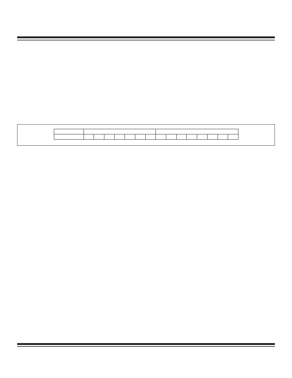
Every MAXQ instruction is encoded as a single 16-bit word according to the format in Figure 2-2.
Bit 15 (f) indicates the format for the source field of the instruction as follows:
• If f equals 0, the instruction is an immediate source instruction, and the source field represents an immediate 8-bit value.
• If f equals 1, the instruction is a register source instruction, and the source field represents the register that the source value will be
read from.
Bits 0 to 7 (ssssssss) represent the source for the transfer. Depending on the value of the format field, this can either be an immediate
value or a source register. If this field represents a register, the lower four bits contain the module specifier and the upper four bits con-
tain the register index in that module.
Bits 8 to 14 (ddddddd) represent the destination for the transfer. This value always represents a destination register, with the lower four
bits containing the module specifier and the upper three bits containing the register sub-index within that module.
Since the source field is 8 bits wide and 4 bits are required to specify the module, any one of 16 registers in that module may be spec-
ified as a source. However, the destination field has one less bit, which means that only eight registers in a module can be specified
as a destination in a single-cycle instruction.
While the asymmetry between source and destination fields of the op code may initially be considered a limitation, this space can be
used effectively. Firstly, since read-only registers will never be specified as destinations, they can be placed in the second eight loca-
tions in a module to give single-cycle read access. Secondly, there are often critical control or configuration bits associated with sys-
tem and certain peripheral modules where limited write access is beneficial (e.g., watchdog-timer enable and reset bits). By placing
such bits in one of the upper 24 registers of a module, this write protection is added in a way that is virtually transparent to the assem-
bly source code. Anytime that it is necessary to directly select one of the upper 24 registers as a destination, the prefix register PFX is
used to supply the extra destination bits. This prefix register write is inserted automatically by the assembler and requires one addi-
tional execution cycle.
The MAXQ architecture is transport-triggered. This means that writing to or reading from certain register locations will also cause side
effects to occur. These side effects form the basis for the higher level op codes defined by the assembler, such as ADDC, OR, JUMP,
and so on. While these op codes are actually implemented as MOVE instructions between certain register locations, the encoding is
handled by the assembler and need not be a concern to the programmer. The registers defined in the System Register and Peripheral
Register maps operate as described in the documentation; the unused "empty" locations are the ones used for these special cases.
The MAXQ instruction set is designed to be highly orthogonal. All arithmetic and logical operations that use two registers can use any
register along with the accumulator. Data can be transferred between any two registers in a single instruction.
Figure 2-2. Instruction Word Format
FORMAT
DESTINATION
SOURCE
f
d
d
d
d
d
d
d
s
s
s
s
s
s
s
s
Maxim Integrated